8
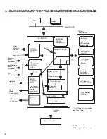
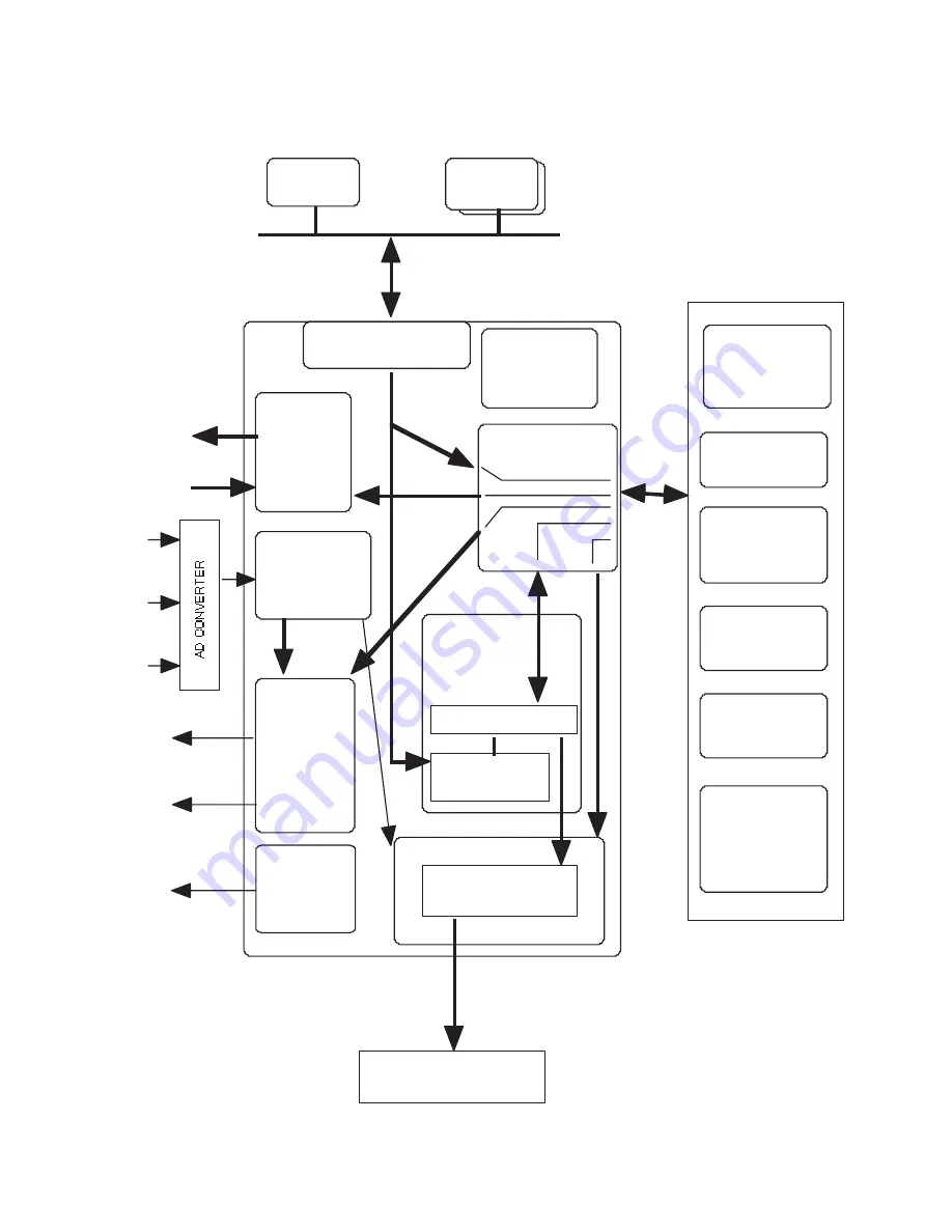
4. BLOCK DIAGRAM OF THE FPGA CIRCUMFERENCE ON A MAIN BOARD
TPH I/F BLOCK
Line Buffer Memory
x 2
Thermal Print Head
Print Data
Strobe
Lutch
SDRAM
4MWordx16bit
16bit
Data
Plane Memory
2MByte
Step Motor
Speed Up/Down
Table
(CPU generates
the table data.)
Heater control
Table(*2)
TPH Control
Table(*2)
(Strobe)
Tables for
Print Data
Correction(*2)
Work Memory
for PRINT BLOCK
(*1)(*2)These data are copied
from Flash Memory.
CPU I/F BLOCK
32bit CPU BUS
16bit
Data
CPU
Flash
Memory
AD
CONVERTER
CONTROL
BLOCK
SDRAM I/F BLOCK
HEATER
CONTROL
BLOCK
(The Heaters
are controlled
by each
temperature.)
PRINT BLOCK
(Temperature
correction,
Outline emphasis,
LUT)
MOTOR
CONTROL
BLOCK
INTERNAL
CLOCK
GENERATOR
Microcode
Memory(*1)
512Word x 16bit
Data Processor
Sensor input
Motor
Solenoid
Control
Signals
Retransfer
Heater
Control Signal
Bend Remedial
Heater
Control Signal
Retransfer
Heater
Temperature
Bend Remedial
Heater
Temperature
TPH
Temperature
8
9
7
7 8
6
1
2
9
6
5
4
3
2
1
3
5 6
4
D/A
Interface
INK Sensor
LED Driver
*
FPGA =
Field Prgramble Gate Array


