background image

dimtel

dimtel

5.3

Display Panels

5.3.3

Coefficients Panel

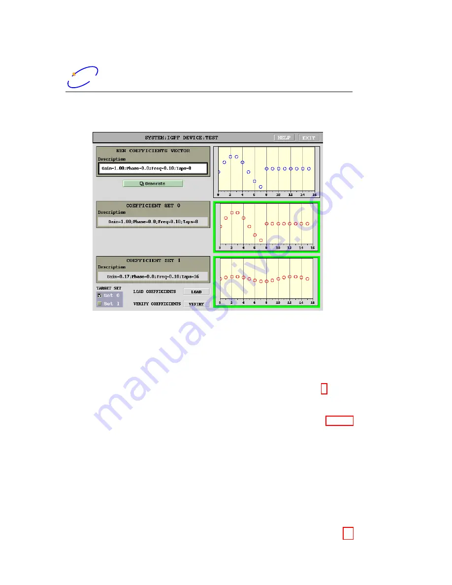
Figure 7: Coefficients panel

Coefficients control panel allows the user to manipulate the loaded coef-

ficients sets and verify that the hardware is in sync with the panel display.
The panel is split into three functional groups: new coefficients vector, coef-
ficient set 0, and coefficient set 1. The first group shows the coefficient vector
and its description generated using coefficient generator panel (Fig. 8). This
vector can be loaded into hardware coefficient sets 0 or 1. Colored borders
around the hardware coefficient displays indicate the results of coefficient
verification. Green shows that the readback is in agreement with the EPICS
values.

Generate

Opens the coefficient generator panel.

TARGET SET

Selects which set the new coefficient vector is to be loaded.

LOAD COEFFICIENTS

Loads the new vector to the hardware coeffi-

cient set specified by

TARGET SET

.

VERIFY

Verifies coefficient sets 0 and 1 against hardware values.

21 of 58

Summary of Contents for iGp-5120F

Page 1: ...iGp 5120F Signal Processor Technical User Manual Author Dmitry Teytelman Revision 1 6 September 19 2008...

Page 2: ...mation in this document is subject to change without notice Copyright Dimtel Inc 2007 All rights reserved Dimtel Inc 2059 Camden Avenue Suite 136 San Jose CA 95124 Phone 1 650 862 8147 Fax 1 603 907 0...

Page 3: ...t 13 5 User Interface 16 5 1 Installation 16 5 2 Starting the EDM 17 5 3 Display Panels 17 5 3 1 Main Panel 17 5 3 2 Control Panel 18 5 3 3 Coefficients Panel 21 5 3 4 Coefficient Generator Panel 22 5...

Page 4: ...egisters 41 9 1 1 Overall Layout 41 9 1 2 Gateware Config Register 42 9 2 Drive pattern memory 44 9 3 Environmental monitor 45 9 4 MAX1202 8 channel ADC 46 9 5 AD8842 8 channel DAC 47 9 6 ECL delay li...

Page 5: ...nside Do not operate with the cover removed Refer to qualified personnel for service NOTE This equipment has been tested and found to comply with the limits for a Class A digital device pursuant to Pa...

Page 6: ...SMA cable 6 Compact disk with software and documentation 7 User manual 8 CE declaration of conformity 2 2 System Overview ADC Acquisition memory supply monitoring Temperature and Input interface USB...

Page 7: ...consists of a high speed analog to digital converter ADC a field programmable gate array FPGA and a high speed DAC and is driven by the radio frequency RF clock In addition to performing real time co...

Page 8: ...bit resolution 4 Fast ADC Two SMA connectors accept the differential inputs for the high speed ADC When a single input is used the full scale FS swing is 195 mV peak to peak Differential mode swing is...

Page 9: ...f the signal processing digital clock man ager DCM Green locked red unlocked FIDUCIAL ERROR Red indication if the fiducial is missing at the wrong frequency or jittering DCM2 LOCK USER1 Lock status of...

Page 10: ...ed protective ground 3 GPIO This 68 pin connector provides 32 low voltage transistor transistor logic LVTTL signals for future expansion 4 PS 2 keyboard Connect PS 2 keyboard for the initial setup of...

Page 11: ...ak to peak 4 Connect a 50 terminator to Ain Fig 2 item 4 5 Connect high speed DAC output s Fig 2 item 10 to the appropriate back end unit 6 If single ended output configuration is used connect a 50 te...

Page 12: ...e computer The iGp 5120F is delivered with the following network configuration IP address 192 168 1 41 Netmask 255 255 255 0 Gateway 192 168 1 254 Configure the remote computer as follows IP address 1...

Page 13: ...correct date using the calendar d Time Set the correct time The initial setting is taken from the current IOC time If you know the current IOC time to be correct press OK quickly to retain the setting...

Page 14: ...gitudinal feedback channels NOTE If the setup program is executed remotely and the network address is changed the ssh connection will hang at the end of the process To connect to the IOC close the exi...

Page 15: ...memories and peripherals In order to perform the testing system hardware must be configured as follows Connect the 16 pin ribbon cable between the 7 channel DAC Fig 2 item 2 and the 8 channel ADC Fig...

Page 16: ...AC mV ADC mV 19 1 2040 2062 5 2039 2025 20 2 2024 2039 4 2039 2028 21 3 2035 2039 3 2039 2033 22 4 2029 2039 2 2039 2035 23 5 2025 2039 8 2039 2030 24 6 2033 2039 3 2039 2034 25 7 2031 2039 3 2039 203...

Page 17: ...rinted out in millivolts Next the DAC is set to 0 and the ADC reading offset column 4 is taken Finally the code finds the maximum DAC setting that does not saturate the ADC Lines 27 31 This portion of...

Page 18: ...ither via sudo or su When prompted enter the user name to install under If the specified user does not exist it will be created Default user name is iGp When prompted enter the installation directory...

Page 19: ...ay brings up the top level panel shown in Figure 5 All of the display panels include two buttons on the top HELP and EXIT EXIT button will always close the current window In addition EXIT button on th...

Page 20: ...SAMPLING Processing channel downsampling factor SAT THRESHOLD iGp 5120F is equipped with an integrating satura tion counter The counter is compared with a threshold duty cycle expressed here in percen...

Page 21: ...tion This can be used to delay data acquisition and give slow oscillations time to grow TRIGGER SRC Acquisition trigger source internal or external External trigger is taken from TRIG2 input NIM level...

Page 22: ...S R Configuration save restore panel Clock missing RF clock missing indicator DCM1 unlocked Signal processing DCM lock indicator DCM2 unlocked Data acquisition DCM lock indicator FIR saturation FIR fi...

Page 23: ...nd its description generated using coefficient generator panel Fig 8 This vector can be loaded into hardware coefficient sets 0 or 1 Colored borders around the hardware coefficient displays indicate t...

Page 24: ...t based on sampling a sine wave Transfer function of the filter is computed and displayed together with a adjustable marker GAIN Filter gain in the range from 0 to 1 PHASE Filter phase in degrees FREQ...

Page 25: ...e is handled automatically OUTPUT DELAY High speed DAC output delay in units of RF periods FIDUCIAL DELAY Input fiducial delay in steps of two bunches Use to place bunch 1 signal in channel 1 of the d...

Page 26: ...after installation To do so connect the RF clock and the fiducial in the final operational configuration Then adjust the fidu cial delay to find the error range Let us consider for example RF frequen...

Page 27: ...tput has many applications Back end timing Kicker gain checking Excitation source for front end timing DRIVE ENABLE Switches high speed DAC between the feedback filter output and the drive signal DRIV...

Page 28: ...tructure of this field allows three types of elements single bunch number range range with a step Individual elements should be separated by spaces Single bunch number element is an in teger in the ra...

Page 29: ...last plot is obtained by performing the fast Fourier transform FFT on each of the bunches and quadratically averaging the resulting spectra This plot aliases all coupled bunch eigenmodes to a frequen...

Page 30: ...oughly corresponds to averaging time constant expressed in spectrum updates For example setting this field to 10 produces exponential time constant of 10 seconds at 1 Hz update rate Value of 1 disable...

Page 31: ...pherals inte grated in the iGp 5120F There are four adjustable delay units for controlling the high speed ADC DAC and fiducial timing WARNING While these delay controls can be used to adjust var ious...

Page 32: ...used to trim the output offset of the high speed DAC That setting is preconfigured at the factory and should not be changed From the device control panel one can open four other panels MAX1202 ADC sec...

Page 33: ...tons on the top of the panel one can select one of the two drivers WARNING Front back end driver sets several I O pins as out puts Make sure correct hardware is connected to the GPIO port before selec...

Page 34: ...g is provided as a readout labeled FRONT END PHASE DAC SET TING When the phase servo loop is open the register is directly driven by the front end phase control setpoint Closed phase servo loop adjust...

Page 35: ...timization can be carried out with beam by stepping the input offset and observing the phase servo re sponse using a stripchart tool INPUT OFFSET is used to zero out possible mixer offset or alternati...

Page 36: ...ctions are available line and RF Line power switch turns main power supply on and off That also controls the state of the cooling fans RF control enables actual amplifier operation Both controls will...

Page 37: ...unction reads out the raw data vector from the IOC and returns it to the caller A single argument is the PV root name e g IGPF TEST adctest This function extracts the iGp 5120F data and fits a sinewav...

Page 38: ...al Falling edge trigger NIM level Minimum fiducial pulse width 1 96 ns External trigger inputs 2 inputs NIM level falling edge Minimum trigger pulse width 3 93 ns Data acquisition memory SRAM 8 Msampl...

Page 39: ...eter Definition Coefficients 16 bit wide in Q15 format Coefficient sets 2 Coefficient set select 0 or 1 FIR channel enable control On Off Shift gain 0 to 7 Downsampling 1 to 32 Table 4 Control paramet...

Page 40: ...length Hold off before recording In units of 4 samples 0 to 232 1 Recording downsampling 1 to 32 Table 6 Monitoring and diagnostics Parameter Definition Clock status RF clock missing DCM lock Feedbac...

Page 41: ...ch by bunch drive enable mask Allows any subset of bunches to be driven Frequency range bunch by bunch mode 0 Frf 2 Frequency range turn by turn mode 0 Frev 2 Table 8 Input Power Requirements Paramete...

Page 42: ...e and no other warranty whether written or oral is expressed or implied 8 2 Support Dimtel Inc will provide technical support for the product free of charge for a period of one year from the date of s...

Page 43: ...005 15 0 FIR coefficient 2 set 1 0x000006 15 0 FIR coefficient 3 set 0 0x000007 15 0 FIR coefficient 3 set 1 0x000008 15 0 FIR coefficient 4 set 0 0x000009 15 0 FIR coefficient 4 set 1 0x00000a 15 0 F...

Page 44: ...ware config register 0x107 provides information about the unit s func tionality gateware revision harmonic number and processing demultiplex ing Table 10 FPGA registers control and status Address Bits...

Page 45: ...locked 5 Fiducial error 6 Acquisition DCM unlocked 31 7 Reserved 0x000102 DCM phase shift register 8 0 Phase shift default 0x100 0 deg range 0x80 to 0x180 31 9 Unused read out as 0 0x000104 Output del...

Page 46: ...eserved 0x000109 Acquisition length 20 0 Acquisition length in units of 4 samples 31 21 Reserved 0x000200 Acquisition status read only 0 Acquisition in progress memory busy 31 2 Reserved 0x000201 ADC...

Page 47: ...4 ADC The ADC provides two current sources Iptat and Ipconst for temperature measurement ADC temperature is given by 300Iptat Ipconst 273 In the iGp 5120F the two sources are loaded by 5 1 k resistors...

Page 48: ...rnal diode AIN0 AIN1 0x00011e 15 0 Device 2 External diode AIN2 AIN3 0x00011f 15 0 Device 2 AIN5 AIN5 differential measurement 9 4 MAX1202 8 channel ADC iGp 5120F includes 8 channel 12 bit serial inte...

Page 49: ...are sign extended to 16 bits DAC reference voltage is 3 V for 3 to 3 V output range Output drivers generate full swing into high impedance loads For 50 loads the swing is reduced to 1 V Unlike other D...

Page 50: ...1 and 2 Finally delay line 3 must be adjusted to achieve optimal placement of the DAC clock relative to the FPGA data Table 15 FPGA registers ECL delay lines Address Bits Definition 0x000130 9 0 Delay...

Page 51: ...at the carrier frequency Front and back end attenuation settings are in 0 5 dB steps for a total range of 31 5 dB Table 17 FPGA registers Front back end GPIO Address Bits Definition 0x00013c 11 0 Fro...

Page 52: ...Pin numbering scheme for the 16 pin front panel connectors is shown in Figure 18 Pin definitions for the 7 channel DAC are given in Table 19 and for the 8 channel DAC in Table 20 Table 19 7 channel DA...

Page 53: ...1 14 GND 15 Channel 0 16 GND 68 67 66 65 64 63 62 61 60 59 58 57 56 55 54 53 52 51 50 49 48 47 46 45 44 43 42 41 40 39 38 37 35 36 34 33 32 31 30 29 28 27 26 25 24 23 22 21 20 19 18 17 16 15 14 13 12...

Page 54: ...30 3 Bit 29 4 Bit 28 5 Bit 27 6 Bit 26 7 Bit 25 8 Bit 24 9 Bit 23 10 Bit 22 11 Bit 21 12 Bit 20 13 Bit 19 14 Bit 18 15 Bit 17 16 Bit 16 17 GND 18 Bit 15 19 Bit 14 20 Bit 13 21 Bit 12 22 Bit 11 23 Bit...

Page 55: ...Pin number Definition 34 Bit N C 35 GND 36 GND 37 GND 38 GND 39 GND 40 GND 41 GND 42 GND 43 GND 44 GND 45 GND 46 GND 47 GND 48 GND 49 GND 50 GND 51 GND 52 GND 53 GND 54 GND 55 GND 56 GND 57 GND 58 GN...

Page 56: ...Appendix B Connector Pinouts dimtel dimtel 54 of 58...

Page 57: ...typically used for sampling rate changes decimation and interpolation 34 43 digital to analog converter DAC A hardware device to convert a sequence of digital codes to correspond ing analog voltages o...

Page 58: ...control system EPICS A set of software tools and applications used to develop distributed soft real time control systems 6 10 12 15 16 21 34 57 Ethernet A family of frame based computer networking tec...

Page 59: ...LVTTL inputs only if the latter are 5 V tolerant 8 31 36 NIM NIM originally an acronym for Nuclear Instrumentation Methods logic defines signal levels with 50 termination of 0 V and 0 8 V for logic 0...

Page 60: ...A class of digital circuits built from bipolar junction transistors and resistors TTL defining signal levels VOH 2 4 V VOL 0 4 V VIH 2 V and VIL 0 8 V 57 universal serial bus USB A serial bus standar...

Reviews: