


Dishtronix, Inc.
Dx2400l1 instruction manual rev00.doc 06-10-18 5.14
Page 39/44
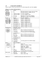
4.1
Block Diagram
Figure 7 shows a block diagram of the DX2400L1 RF Amplifier Deck.
Note that the block diagram includes SO2R (Single Operator, Two Radio) and automatic tuner
modules which are currently not available on the DX2400L1. Future versions of the amplifier
may or may not incorporate these features. It may or may not be possible to retrofit this particular
amplifier.
4.2
Amplifier Circuitry Overview
In the receive or standby mode RF signals are shunted around the amplifier circuit by the input
and output relay and passed through the SWR sensor to the antenna switch assembly, which
connects the transceiver to the selected antenna. If the DX2400 is not activated, Antenna 1 is
connected by default.
Upon being keyed by the transceiver, the output relay changes to the transmit path, connecting
the wattmeter and selected antenna to the output of the filter bank. A short time later, the input
relay changes from the bypass path to connect the transceiver to the amplifier input. Finally bias
to the PA modules is enabled, and if full loop keying is enabled the microprocessor signals the
exciter to begin transmitting. If full loop keying is not selected, the changeover sequence is the
same, except that different timing is used.
Once the transmit path is established, the incoming RF is passed from the input relay to the step
attenuator and leveling circuit to the splitter where the incoming RF is divided into 4 identical
signals 6dB down from the input level. Each of these signals are used to drive identical push pull
broadband power modules operating at 72V.
Each RF power module is matched for gain within a fraction of a dB by an attenuator pack
(nominally -2dB) located on the module input. The transistors in each module are also a gain
matched set. Further, amplifiers are usually built at the factory with all matched transistor sets.
For this reason, replacement of the transistors requires specialized equipment and an assortment
of resistors for the gain compensation attenuator. Dishtronix may provide completely assembled
and gain compensated modules on an exchange basis for field replacement.
Each RF power module is monitored for current that is reported to the microprocessor.
Additionally the RF power module measures the heat sink temperature to report to the
microprocessor.
After amplification in each of the power modules, the four RF signals are passed to the Combiner
Assembly. where the signals are summed to produce the output signal which is 6dB greater than
the individual input levels. Upon exiting the combiner, the amplified signal is passed to the Low
Pass Filter (LPF) assembly.
Upon entering the LPF assembly, the amplified signal is passed through a reflected power sensor
and applied to one of six low pass filters selected by the microprocessor. Should a filter fail or be
incorrectly be selected, or any other failure occur that causes high reflected power, the reflected
power sensor activates the protection circuitry located on the microprocessor circuit board. The
selected filter attenuates the harmonic energy and passes a spectrally clean (with harmonics
typically -50-60 dBc), amplified signal to the amplifier output relay.
Summary of Contents for DX2400L1
Page 11: ...Dishtronix Inc Dx2400l1 instruction manual rev00 doc 06 10 18 5 14 Page 11 44 2 INSTALLATION...
Page 19: ...Dishtronix Inc Dx2400l1 instruction manual rev00 doc 06 10 18 5 14 Page 19 44 3 OPERATION...
Page 41: ...Dishtronix Inc Dx2400l1 instruction manual rev00 doc 06 10 18 5 14 Page 41 44 5 SERVICE...
Page 44: ...Dishtronix Inc Dx2400l1 instruction manual rev00 doc 06 10 18 5 14 Page 44 44 NOTES...


