background image

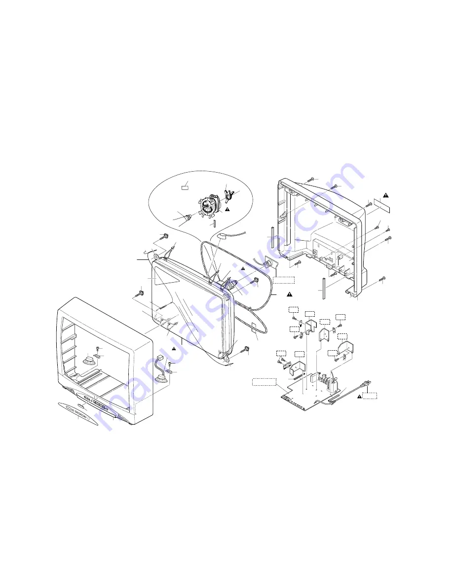
EXPLODED VIEWS

Cabinet

11-1

11-2

L6250CEX

PB6

PB6

A3

A2

A1

L1

L1

B4

B4

SP801

SP802

B2

B2

B5

B5

B2

B1

B2

A6

L2

L2

L2

L2

L4

L2

L2

L3

L2

A5

B-8

B-7

B-6

L-1

L-1

B-9

L-1

L-1

A4

L-1

Scotch Tape #880

MAIN CBA

CRT CBA

AC601

V501

DY551

CLN551

L691

Lead Clamper

Lead Clamper

Lead 
Clamper

Lead 
Clamper

Lead 
Clamper

Lead 
Clamper

V501-1

DY551

Details for DY551 
and surrounding parts

SHINWHA 
TAPE SGT-730
(WHITE)

SHINWHA 
TAPE SGT-730
(BLACK)

V501-2

Summary of Contents for DCT3203

Page 1: ...32 COLOR TELEVISION DCT3203 SERVICE MANUAL ...

Page 2: ...valuate and advice the service trade of all con ceivable ways in which service might be done or of the possible hazardous consequences of each way Consequently Funai has not undertaken any such broad evaluation Accordingly a servicer who uses a service proce dure or tool which is not recommended by Funai must first use all precau tions thoroughly so that neither his safety nor the safe operation o...

Page 3: ...t limit specifications Description Condition Unit Nominal Limit 1 Intermediate Freq Picture Sound MHz MHz 45 75 41 25 2 Peak Picture Sens VHF CATV UHF dBµV dBµV dBµV 15 15 15 30 30 40 3 AFT Pull In Range 10mV input MHz 2 2 0 7 Description Condition Unit Nominal Limit 1 Deflection Freq Horizontal Vertical KHz Hz 15 734 60 2 Linearity Horizontal Vertical 15 10 3 Over Scan 10 4 High Voltage KV 29 Des...

Page 4: ...ngs tied together and touch the other ohmme ter lead in turn to each tuner antenna input ex posed terminal screw and if applicable to the coaxial connector If the measured resistance is less than 1 0 megohm or greater than 5 2 mego hm an abnormality exists that must be corrected before the instrument is returned to the customer Repeat this test with the instrument AC switch in the off position d L...

Page 5: ...the ground side of the AC power source To confirm that the AC power plug is inserted correctly with an AC volt meter measure between the chassis and a known earth ground If a voltage reading in excess of 1 0V is obtained remove and reinsert the AC power plug in the opposite polarity and again measure the voltage potential between the chassis and a known earth ground b Some TV receiver chassis norm...

Page 6: ...replaced wires do not contact sharp edged or pointed parts H When a power cord has been replaced check that 5 6 kg of force in any direction will not loosen it I Also check areas surrounding repaired locations J Use care that foreign objects screws solder drop lets etc do not remain inside the set K Crimp type wire connector The power transformer uses crimp type connec tors which connect the power...

Page 7: ...xposed accessible parts RF terminals an tenna terminals video and audio input and output ter minals microphone jacks earphone jacks etc is lower than or equal to the specified value in the table below Measuring Method Power ON Insert load Z between B earth ground power cord plug prongs and exposed accessible parts Use an AC voltmeter to measure across both terminals of load Z See Fig 2 and followi...

Page 8: ...C is fixed with glue to the CBA when removing entire flat pack IC first apply soldering iron to center of the flat pack IC and heat up Then remove glue will be melted Fig S 1 6 4 Release the flat pack IC from the CBA using twee zers Fig S 1 6 Caution 1 Do not supply hot air to the chip parts around the flat pack IC for over 6 seconds because damage to the chip parts may occur Put masking tape arou...

Page 9: ... pins of the flat pack IC you can remove it easily Fig S 1 3 2 Affix the wire to a workbench or solid mounting point as shown in Fig S 1 5 3 While heating the pins using a fine tip soldering iron or hot air blower pull up the wire as the solder melts so as to lift the IC leads from the CBA con tact pads as shown in Fig S 1 5 4 Bottom of the flat pack IC is fixed with glue to the CBA when removing ...

Page 10: ...cur due to a potential difference caused by electro static charge during unpacking or repair work 1 Ground for Human Body Be sure to wear a grounding band 1MΩ that is prop erly grounded to remove any static electricity that may be charged on the body 2 Ground for Workbench Be sure to place a conductive sheet or copper plate with proper grounding 1MΩ on the workbench or other surface where the semi...

Page 11: ...sed unplugged unclamped or desoldered S Screw P Spring L Locking Tab CN Con nector Unhook Unlock Release Unplug or Desolder 2 S 2 two Screws S 2 5 Refer to the following Reference Notes in the Table Reference Notes in the Table 1 Removal of the Rear Cabinet Remove screws 7 S 1 1 S 2 and 3 S 4 then slide the Rear Cab inet backward 2 Removal of the CRT CBA Disconnect CN1501 then pull the CRT CBA bac...

Page 12: ...4 2 L6655DC Fig 1 S 1 S 2 S 4 1 Rear Cabinet S 1 S 1 S 1 Fig 2 1 Rear Cabinet S 1 S 1 S 1 S 1 S 1 S 1 S 1 S 4 S 2 3 Main CBA Fig 3 Fig 4 4 CRT Anode Cap S 3 S 3 S 3 S 3 ...

Page 13: ...iring Diagram CN691 ANODE CN801 CLN801 SP801 L691 DEGAUSSING COIL MAIN CBA FLYBACK TRANSFORMER T571 AC601 AC CORD TU1 TUNER WH501B WH301B FOCUS SCREEN WH501A WH301A TO CRT GROUND CN571 CN1501 JK1501 CN802 CLN802 SP802 Fig 5 ...

Page 14: ...ig 1 2 Notes 1 The service remote control unit that be made in above method is usable in the electrical adjust ment of the following models SRT2313 2319 SRT2213B 2219B SRT2227X SRT2223X SRT2223B SRT2232X SRT2220P SRT4127P 2 The attached remote control unit can not be used as service remote control unit How to set up the service mode Service mode 1 Use the service remote control unit 2 Turn the pow...

Page 15: ...EO Set to V1 V2 AV MEMO Set to ON STABLE SOUND Set to OFF FILTER Set to ON Adjusting the monitoring time Set to 500 YUV MEMORY Set to OFF 3 AV Memory Setting data General 1 Enter the Service mode See page 5 1 2 When AV MEMORY setting to ON refer to 2 Initial Setting press VOL o button on the ser vice remote control unit Display changes SPORT CNT SPORT CLR SPORT SRP NEWS CNT NEWS CLR NEWS SRP MOVIE...

Page 16: ...the value of S COLOR S CLR becomes 56 TNT 1 Press MENU button on the service remote con trol unit Then select TINT TNT display 2 Press CH o p buttons on the service remote control unit so that the value of TINT TNT be comes 62 V TNT 1 Press MENU button on the service remote con trol unit Then select V TINT V TNT display 2 Press CH o p buttons on the service remote control unit so that the value of...

Page 17: ... Purity Check 1 Enter the Service mode See page 5 1 2 Press 7 button on the remote control unit Each time pressing 7 button on the remote control unit display changes Red mode Green mode Blue mode and White mode cyclically 3 Select White mode 4 Turn the power off and on again Main power but ton on the TV unit 7 SD Check Mode 1 Enter the Service mode See page 5 1 2 Press 1 button on the remote cont...

Page 18: ...off and on again Main power but ton on the TV unit 10 V Position Adjustment Purpose To obtain correct vertical width of screen image Symptom of misadjustment If V Position is incor rect vertical height of image on the screen may not be properly displayed Note Use service remote control unit 1 Operate the unit for at least 20 minutes 2 Enter the Service Mode See page 5 1 3 Receive the monoscope pat...

Page 19: ...size of image on the screen may not be properly displayed Note Use service remote control unit 1 Operate the unit for at least 20 minutes 2 Receive the Monoscope Pattern 3 Adjust VR562 so that the monoscope pattern will be 90 5 of display size and circle is round 4 Turn the Power off and on again Main power but ton on the TV unit 15 PIN Cushion Adjustment Purpose To obtain correct straight vertica...

Page 20: ...s correctly for pure white Symptom of Misadjustment White becomes bluish or reddish Note Use service remote control unit 1 Operate the unit more than 20 minutes 2 Face the unit to east Degauss the CRT using De gaussing Coil 3 Input the White Raster APL 100 4 Set the color analyzer to the CHROMA mode and after zero point calibration bring the optical recep tor to the center on the tube surface CRT ...

Page 21: ...clear picture The following adjustments normally are not attempted in the field Only when replacing the CRT then adjust as a preparation 20 Purity Adjustment Purpose To obtain pure color Symptom of Misadjustment If Color Purity Adjust ment is incorrect large areas of color may not be properly displayed 1 Set the unit facing east 2 Operate the unit for over 30 minutes before adjust ing 3 Fully dega...

Page 22: ... rotating RB G C P Magnet See Fig 8 3 Paintlock the C P Magnets after adjustment 4 Remove the DY Wedges and slightly tilt the De flection Yoke horizontally and vertically to obtain the best overall convergence 5 Fix the Deflection Yoke by carefully inserting the DY Wedges between CRT and Deflection Yoke Test Point Adj Point Mode Input C P Magnet RB C P Magnet RB G Deflection Yoke Dot Pattern or Cr...

Page 23: ...SUPPLY BLOCK FROM TO CRT H V BLOCK PROTECT 2 PROTECT 1 PROTECT 3 P ON H P ON H KEY IN2 KEY IN1 RCV IN RCV101 IC151 MEMORY SCL 6 SDA 5 VOLUME 67 68 76 79 69 66 70 PROTECT 2 PROTECT 1 SDA 5 I2C OPEN 3 SCL 6 CN301 NO CONNECTION CN301 is used for adjustment at factory 7 CS 72 I2C OPEN IC333 TV MICON VIDEO AUDIO CHROMA DEFLECTION FROM IF VIDEO BLOCK INPUT0 TO IF VIDEO BLOCK TO AUDIO BLOCK VOLUME 64 A M...

Page 24: ...SW CONTRAST BRIGHTNESS RGB DRIVE CUT OFF H V BLK LPF 14 20 29 11 61 53 46 45 38 37 ACL H DRIVE FBP RAMP OUT V RAMP F B JK721 VIDEO IN 24 SAW FILTER VIF AMP VIDEO DET VCO 4 5MHz FILTER LPF IF AGC DET EQ AMP RF AGC AMP AFT 4 5MHz TRAP SIF AMP 20 14 16 22 7 21 5 3 8 1 10 TU1 SF1 IF AGC SDA SCL EXT CLK 1 11 5 4 8 17 26 SIF 52 51 50 MAIN CBA VIDEO SIGNAL RF IF SIGNAL AUDIO SIGNAL JK701 VIDEO IN WF16 WF...

Page 25: ... L R FILTER WIDE BAND FILTER WIDE BAND RMS DET WIDE BAND EXPAND SPECTRAL EXPAND SPECTRAL RMS DET SPECTRAL FILTER OFFSET CANCEL L CH R CH MATRIX AGC OFFSET CANCEL L R FILTER L R SAP SW SAP FILTER I2C DECORDER SAP DEMOD SAP OUT FILTER 29 30 FROM IF VIDEO BLOCK TUNER REAR FRONT TUNER REAR FRONT L CH R CH 21 27 24 IC431 MTS SAP AUDIO SIGNAL PROCESS AUDIO IN L REAR JK702 SIF JK703 IC801 AUDIO AMP 6 7 2...

Page 26: ...B WH501A VIDEO SIGNAL CN551 H OUTPUT H DRIVE B 15kHz TP302 GND TP500 BLUE TP501 X RAY CHECK TP591 TP592 PROTECT 3 DEF B AMP 7 1 Q533 6 3 PULSE UP THERMAL PROTECTION SWITCHING P ON ON 5 SWITCHING SWITCHING WF7 WF8 WF11 WF12 WF9 WF10 WF3 WF15 WF4 WF14 WF5 WF13 RED AMP PROTECT 2 RED 3 GREEN 4 BLUE 5 HEATER 3 3 200V 1 1 PROTECT 1 H CONTROL FROM POWER SUPPLY BLOCK FROM TO IF VIDEO BLOCK FROM TO SYSTEM ...

Page 27: ...OF IC333 Q682 P ON 5V 5V CTRL FROM PIN28 OF IC333 Q683 5V SWITCHING 5V SWITCHING 5V SWITCHING AL 9V Q321 9V SWITCHING Q674 SWITCHING P ON ON P ON H FROM PIN79 OF IC333 Q832 SWITCHING P ON ON SWITCHING P ON ON HOT CIRCUIT BE CAREFUL FOR CONTINUED PROTECTION AGAINST RISK OF FIRE REPLACE ONLY WITH SAME TYPE 4 A 125V FUSE CAUTION ATTENTION UTILISER UN FUSIBLE DE RECHANGE DE MÊME TYPE DE 4A 125V 4A 125...

Page 28: ...wings for ordering The correct part number is shown in the parts list and may be slightly different or amended since these drawings were prepared 2 All resistance values are indicated in ohms K 103 M 106 3 Resistor wattages are 1 4W or 1 6W unless otherwise specified 4 All capacitance values are indicated in µF P 10 6 µF 5 All voltages are DC voltages unless otherwise specified Note of Capacitors ...

Page 29: ...aired units use only original replacement parts which are listed with their part numbers in the parts list section of the service manual 4 Wire Connectors 1 Prefix symbol CN means connector can disconnect and reconnect 2 Prefix symbol CL means wire solder holes of the PCB wire is soldered directly 5 Note Mark I is a leadless chip component 6 Voltage indications on the schematics are as shown below...

Page 30: ...3 C4 D1 D2 D3 D4 E1 E2 E3 E4 F1 F2 F3 F4 VIDEO SIGNAL Main 1 4 Schematic Diagram 7 3 7 4 L6655SCM1 MAIN 1 4 Ref No Position IC151 A 3 IC333 C 2 Q111 D 1 Q131 A 3 Q141 A 4 Q191 B 4 Q192 B 4 Q321 E 2 CN301 A 3 ICS TRANSISTORS CONNECTOR ...

Page 31: ...K4 L1 L2 L3 L4 VIDEO SIGNAL AUDIO SIGNAL 7 5 7 6 L6655SCM2 Main 2 4 Schematic Diagram MAIN 2 4 Ref No Position IC431 G 3 IC771 H 2 IC801 J 4 Q825 J 3 Q831 K 3 Q832 K 3 Q841 K 3 Q851 J 3 Q951 H 1 Q956 H 1 Q961 J 3 CN801 L 4 CN802 L 3 TRANSISTORS CONNECTORS ICS ...

Page 32: ... 4 Schematic Diagram CAUTION Fixed voltage or Auto voltage selectable power supply circuit is used in this unit If Main Fuse F601 is blown check to see that all components in the power supply circuit are not defective before you connect the AC plug to the AC power supply Otherwise it may cause some components in the power supply circuit to fail MAIN 3 4 Ref No Position IC33 P 3 IC601 O 1 Q21 P 4 Q...

Page 33: ...1 U 2 Q572 T 2 TP592 U 2 Q531 S 2 TP601 U 2 Q533 S 2 CN571 T 3 Q547 U 2 WH301A V 2 VR561 U 3 Q551 T 3 WH501A V 3 VR562 U 3 Q552 T 3 Q561 U 3 TP302 V 2 VARIABLE RESISTORS TEST POINTS IC TRANSISTORS TRANSISTORS TEST POINTS CONNECTORS CRT Ref No Position Q1511 W 1 Q1512 W 2 Q1521 W 1 Q1522 W 2 Q1531 W 1 Q1532 W 2 CN1501 X 2 WH301B V 2 WH501B V 3 TP500 W 1 TP501 W 2 CONNECTORS TEST POINTS TRANSISTORS ...

Page 34: ...power supply circuit is used in this unit If Main Fuse F601 is blown check to see that all components in the power supply circuit are not defective before you connect the AC plug to the AC power supply Otherwise it may cause some components in the power supply circuit to fail MAIN CBA Ref No Position Ref No Position IC33 B 2 Q681 D 3 IC151 E 5 Q682 D 4 IC333 F 5 Q683 D 4 IC431 A 1 Q696 D 4 IC551 C...

Page 35: ...ISOLATION TRANSFORMER IS REQUIRED NOTE The voltage for parts in hot circuit is measured using hot GND as a common terminal CAUTION FOR CONTINUED PROTECTION AGAINST RISK OF FIRE REPLACE ONLY WITH SAME TYPE 4A 125V FUSE ATTENTION UTILISER UN FUSIBLE DE RECHANGE DE MÊME TYPE DE 4A 125V 4A 125V 7 13 7 14 BL6650F01011 1 CAUTION Fixed voltage or Auto voltage selectable power supply circuit is used in th...

Page 36: ...31 Collector Q1531 Base WF5 GND TP500 BLUE TP501 7 15 BL6650F01011 2 7 16 CRT CBA Top View CRT CBA Bottom View CRT CBA Ref No Position Q1511 C 1 Q1512 C 1 Q1521 C 1 Q1522 C 1 Q1531 B 1 Q1532 B 1 CN1501 A 2 WH301B B 2 WH501B A 2 TP500 B 2 TP501 B 2 TEST POINTS TRANSISTORS CONNECTORS ...

Page 37: ...F4 1DIV 2V 20µsec Q 1531 Base WF5 GND 1DIV 10V 20µsec Q 572 Collector WF7 GND 1DIV 5V 20µsec Q 571 Base WF8 1DIV 20V 20µsec Q 1531 Collector WF13 1DIV 20V 20µsec Q 1511 Collector WF15 1DIV 0 2V 20µsec TU 1 Pin 8 WF16 GND L6650WF WF1 WF16 Waveforms to be observed at Waveform check points Shown in Schematic Diagram Input NTSC Color Bar Signal with 1kHz Audio Signal INITIAL POSITION Unplug unit from ...

Page 38: ...GND RED GREEN BLUE V501 CRT ANODE L CH R CH 1 SP L 2 SP801 SPEAKER CN801 1 SP R 2 SP802 SPEAKER CN802 9 1 L6655WI T571 FBT TU1 TUNER UNIT WH501A WH501B 8V GND RED GREEN BLUE 8V HEATER 3 GND 2 200V 1 GND 2 200V 1 HEATER 3 CLN801 CLN802 SP GND SP GND BL6650F01011 2 CN301 NO CONNECTION CN301 IS USED FOR ADJUSTMENT AT FACTORY INT MONI 1 AGC 2 I2C OPEN 3 GND 4 SDA 5 SCL 6 ...

Page 39: ... VCC DC 8 7V Input 32 FSC OUT Clock Output 3 58MHz 33 MONITOR OUT Monitor Out 34 N U Not Used 35 N U Not Used 36 N U Not Used 37 V RAMP F B V Ramp Feed Back 38 V RAMP OUT Vertical Output 39 V RAMP CAP V Ramp OSC Capacitor 40 8 7 VREG OUT DC 8 7V Output 41 N U Not Used 42 H VCO F B H Vco Feed Back 43 AFC FILT Horizontal AFC Filter 44 GND GND 45 FBP IN Flyback Pulse Input 46 H OUT H Pulse Output 47 ...

Page 40: ...ite Balance Adjustment Judgement 73 AFT AFT Voltage Input 74 DG ON H Degaussing Coil Control 75 AGC AGC Voltage Input 76 PROTECT 3 Power Supply Protection 77 N U Not Used 78 FM SW Switching IF IC VCO 79 P ON H Output for P ON H 80 INPUT 1 Input Select 1 Pin No Signal Name Function ...

Page 41: ...2 L2 L4 L2 L2 L3 L2 A5 B 8 B 7 B 6 L 1 L 1 B 9 L 1 L 1 A4 L 1 Scotch Tape 880 MAIN CBA CRT CBA AC601 V501 DY551 CLN551 L691 Lead Clamper Lead Clamper Lead Clamper Lead Clamper Lead Clamper Lead Clamper V501 1 DY551 Details for DY551 and surrounding parts SHINWHA TAPE SGT 730 WHITE SHINWHA TAPE SGT 730 BLACK V501 2 ...

Page 42: ...FRONT S2 S6 PACKING TAPE S5 S4 S3 S2 POP LABEL X2 X4 X3 TAPE X1 S1 Packing 11 3 L6250PEX ...

Page 43: ...0 L2 SCREW P TIGHT 4X18 BIND HEAD GBMP4180 L3 SCREW TAPPING M4X14 DBU14140 L4 SCREW P TIGHT 3X10 BIND HEAD GBKP3100 L691 DEGAUSSING COIL F 047 LLBH00ZTM047 PACKING S1 CARTON L6655CF 0EM408289 S2 STYROFOAM TOP ASSEMBLY L6250UA 0EM407000 S3 STYROFOAM BOTTOM ASSEMBLY L6250UA 0EM407001 S4 SET SHEET PCEC 003502019816 0EM403887 S5 SERIAL NO LABEL L6655CF S6 HOLD PAD L6250UA 0EM407005 S7 LABEL EAS H3761U...

Page 44: ...100µF 10V M CE1AMASDL101 C54 CERAMIC CAP AX B K 1000pF 50V CCA1JKT0B102 C55 CERAMIC CAP AX F Z 0 01µF 25V CDA1EZT0F103 C57 FILM CAP P 0 047µF 50V J or CMA1JJS00473 FILM CAP P 0 047µF 50V J or CA1J473MS029 FILM CAP P 0 047µF 50V J TV or CMB1JJS00473 MYLAR CAP 0 047µF 50V K 2250473S C58 FILM CAP P 0 033µF 50V J or CMA1JJS00333 FILM CAP P 0 033µF 50V J or CA1J333MS029 FILM CAP P 0 033µF 50V J TV CMB1...

Page 45: ...LYTIC CAP 10µF 50V M or CE1JMASTL100 ELECTROLYTIC CAP 10µF 50V M CE1JMASDL100 C442 ELECTROLYTIC CAP 2 2µF 50V M or CE1JMASTL2R2 ELECTROLYTIC CAP 2 2µF 50V M CE1JMASDL2R2 Ref No Description Part No C444 ELECTROLYTIC CAP 0 33µF 50V M or CE1JMASTLR33 ELECTROLYTIC CAP 0 33µF 50V M CE1JMASDLR33 C445 FILM CAP P 0 1µF 50V J or CMA1JJS00104 FILM CAP P 0 1µF 50V J or CA1J104MS029 FILM CAP P 0 1µF 50V J TV ...

Page 46: ...100µF 160V M CE2CMZPDL101 Ref No Description Part No C657 ELECTROLYTIC CAP 2200µF 35V M or CE1GMZNTL222 ELECTROLYTIC CAP 2200µF 35V M CE1GMZNDL222 C658 ELECTROLYTIC CAP 1000µF 16V M VR HC or CE1CMZNTL102 ELECTROLYTIC CAP 1000µF 16V M or CE1CMZNDL102 ELECTROLYTIC CAP 1000µF 16V M CE1CMZADL102 C661 CERAMIC CAP AX F Z 0 01µF 25V CDA1EZT0F103 C662 ELECTROLYTIC CAP 1000µF 25V M or CE1EMZNTL102 ELECTROL...

Page 47: ... DIODE 1SS133 T 77 or QDTZ001SS133 SWITCHING DIODE 1N4148 or NDTZ001N4148 DIODE 1SS176TPA7 1SS176T D501 DIODE FR104 B or NDLZ000FR104 Ref No Description Part No RECTIFIER DIODE ERA22 02 or QDPZ0ERA2202 RECTIFIER DIODE 10ELS2 QDQZ0010ELS2 D502 ZENER DIODE MTZJT 7724B or QDTB00MTZJ24 ZENER DIODE DZ 24BSBT265 NDTB00DZ24BS D503 SWITCHING DIODE 1SS133 T 77 or QDTZ001SS133 SWITCHING DIODE 1N4148 or NDTZ...

Page 48: ...IODE MTZJT 776 2B or QDTB0MTZJ6R2 ZENER DIODE DZ 6 2BSBT265 NDTB0DZ6R2BS D851 ZENER DIODE MTZJT 7712B or QDTB00MTZJ12 ZENER DIODE DZ 12BSBT265 NDTB00DZ12BS Ref No Description Part No D853 ZENER DIODE MTZJT 779 1B or QDTB0MTZJ9R1 ZENER DIODE DZ 9 1BSBT265 NDTB0DZ9R1BS D854 SWITCHING DIODE 1SS133 T 77 or QDTZ001SS133 SWITCHING DIODE 1N4148 or NDTZ001N4148 DIODE 1SS176TPA7 1SS176T D855 SWITCHING DIOD...

Page 49: ...785 H or QQSH02SC2785 TRANSISTOR 2SC2785 J or QQSJ02SC2785 TRANSISTOR KTC3199 GR or NQS10KTC3199 Ref No Description Part No TRANSISTOR KTC3198 GR or NQS40KTC3198 TRANSISTOR 2SC3331 T AANP or 2SC3331TZ TRANSISTOR 2SC3331 U AANP or 2SC3331UZ TRANSISTOR 2SC1815 GR TPE2 QQS102SC1815 Q551 TRANSISTOR 2SA1175 F or QQSF02SA1175 TRANSISTOR KTA1267 GR or NQS10KTA1267 TRANSISTOR KTA1266 GR or NQS40KTA1266 TR...

Page 50: ...W J 100k Ω RCX4JATZ0104 Ref No Description Part No R43 CARBON RES 1 4W J 12k Ω RCX4JATZ0123 R44 CARBON RES 1 4W J 100 Ω or RCX4JATZ0101 CARBON RES 1 6W J 100 Ω RCX6JATZ0101 R51 CARBON RES 1 4W J 220k Ω RCX4JATZ0224 R52 CARBON RES 1 4W J 220k Ω RCX4JATZ0224 R54 CARBON RES 1 4W J 22k Ω RCX4JATZ0223 R102 CARBON RES 1 4W J 1 5k Ω RCX4JATZ0152 R103 CARBON RES 1 4W J 2 2k Ω RCX4JATZ0222 R104 CARBON RES ...

Page 51: ...or RCX4JATZ0681 CARBON RES 1 6W J 680 Ω RCX6JATZ0681 Ref No Description Part No R520 CARBON RES 1 4W J 22k Ω RCX4JATZ0223 R522 CARBON RES 1 4W J 22k Ω RCX4JATZ0223 R531 CARBON RES 1 4W J 1 8k Ω RCX4JATZ0182 R532 CARBON RES 1 4W J 22k Ω RCX4JATZ0223 R533 CARBON RES 1 4W J 22k Ω RCX4JATZ0223 R534 CARBON RES 1 4W J 22k Ω RCX4JATZ0223 R535 CARBON RES 1 4W J 470 Ω or RCX4JATZ0471 CARBON RES 1 6W J 470 ...

Page 52: ... 4W J 15k Ω RCX4JATZ0153 R678 CARBON RES 1 4W J 47k Ω RCX4JATZ0473 R679 CARBON RES 1 4W J 3 3k Ω RCX4JATZ0332 Ref No Description Part No R680 CARBON RES 1 4W J 10k Ω RCX4JATZ0103 R681 CARBON RES 1 4W J 12 Ω or RCX4JATZ0120 CARBON RES 1 6W J 12 Ω RCX6JATZ0120 R682 METAL OXIDE FILM RES 2W J 33 Ω or RN02330ZU001 METAL OXIDE FILM RES 2W J 33 Ω RN02330DP004 R683 METAL RESISTOR 2W J 39 Ω or RN02390ZU001...

Page 53: ...ption Part No BC571 BEAD INDUCTORS FBA04HA600VB 00 LLBF00STU026 BC572 PCB JUMPER D0 6 P5 0 JW5 0T BC602 PCB JUMPER D0 6 P5 0 JW5 0T BC603 BEAD INDUCTORS FBR07HA121TB 00 LLBF00ZTU021 BC652 BEAD INDUCTORS FBR07HA121TB 00 LLBF00ZTU021 BC653 PCB JUMPER D0 6 P5 0 JW5 0T BC654 BEAD INDUCTORS FBR07HA121TB 00 LLBF00ZTU021 BC655 BEAD INDUCTORS FBR07HA121TB 00 LLBF00ZTU021 BC656 BEAD INDUCTORS FBR07HA121TB ...

Page 54: ...iption Part No L1531 PCB JUMPER D0 6 P5 0 JW5 0T TRANSISTORS Q1511 TRANSISTOR 2SC2785 F or QQSF02SC2785 TRANSISTOR 2SC2785 H or QQSH02SC2785 TRANSISTOR 2SC2785 J or QQSJ02SC2785 TRANSISTOR KTC3199 GR or NQS10KTC3199 TRANSISTOR KTC3198 GR or NQS40KTC3198 TRANSISTOR 2SC3331 T AANP or 2SC3331TZ TRANSISTOR 2SC3331 U AANP or 2SC3331UZ TRANSISTOR 2SC1815 GR TPE2 QQS102SC1815 Q1512 TRANSISTOR 2SC5360 or ...

Page 55: ...001 FIXED METAL OXIDE FILM RES 3W J 10k Ω RN03103DP005 R1531 CARBON RES 1 4W J 1 5k Ω RCX4JATZ0152 R1532 CARBON RES 1 4W J 1 5k Ω RCX4JATZ0152 R1534 CARBON RES 1 4W J 100 Ω or RCX4JATZ0101 CARBON RES 1 6W J 100 Ω RCX6JATZ0101 R1535 CARBON RES 1 4W J 820 Ω or RCX4JATZ0821 CARBON RES 1 6W J 820 Ω RCX6JATZ0821 R1538 CARBON RES 1 4W J 220 Ω or RCX4JATZ0221 CARBON RES 1 6W J 220 Ω RCX6JATZ0221 MISCELLA...

Page 56: ...DCT3203 L6655CF ...

Reviews: