background image

T5L_ASIC Development Guide


- 3 - 

www.dwin-global.com 


DWIN Technology 

Professional, 

Creditable, 

S

uccessful


1 Summary


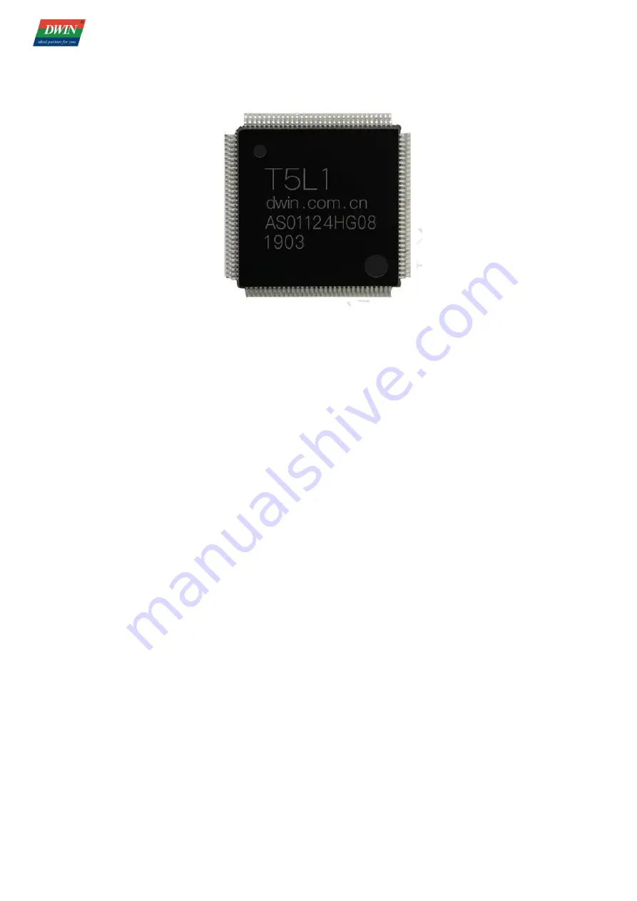
The T5L series ASIC is a single-chip and dual-core ASIC designed by DWIN technology co., ltd for 

AIOT  applications  with  low  power  consumption,  high  cost  performance,  GUI  and  highly integrated 

application, including T5L1(low resolution) and T5L2(high resolution). Its main features are as follow: 

(1)  Mature  and  stable  8051  core  which  is  the  most  widely  used  with  the  maximum  operating 

frequency of T5L is up to 250MHz, 1T(single instruction cycle)high speed operation. 

(2)  Separated GUI CPU core running DGUS II System: 


High-speed  display  memory,  2.4GB/S  bandwidth,  24bit  color  display  resolution  supporting  to 

800*600(T5L1) or 1366*768(T5L2). 


2D hardware acceleration, the decompression speed of JPEG is up to 200fps@1280*800, the 

UI with animation and icons as its main feature is extremely cool and smooth. 


Images and icons stored in JPEG format. Adopt Low-cost 16Mbytes SPI Flash. 


Support CTP or RTP with adjustable sensitivity and maximum 400Hz touch frequency. 


High-quality speech compression storage and playback. 


128Kbytes variable storage space for exchanging data with OS CPU core and memory  


1-way  15bit  32Ksps  PWM  digital  power  amplifier  driver  loudspeaker  to  save  power  amplifier 

cost and achieve high signal-to-noise ratio and sound quality restoration. 


Support DGUS development and simulation on PC. Support background remote upgrade. 

(3)  Separated CPU (OS CPU) core runs user 8051 code or DWIN OS system, user CPU omitted in 

practical application. 

Summary of Contents for T5L ASIC Series

Page 1: ...T5L_ASIC Development Guide 1 www dwin global com DWIN Technology Professional Creditable Successful T5L_ASIC Development Guide Version 2 0 2022 4 13...

Page 2: ...iguration 14 3 2 Memory 15 3 2 1 Code Memory 64KBytes 15 3 2 2 Variable Memory 256KBytes 16 3 2 3 Data Memory 32KBytes 18 3 2 4 Extended SFR Register 19 3 3 Mathematical Operating Unit MDU 20 3 4 Time...

Page 3: ...r display resolution supporting to 800 600 T5L1 or 1366 768 T5L2 2D hardware acceleration the decompression speed of JPEG is up to 200fps 1280 800 the UI with animation and icons as its main feature i...

Page 4: ...curity 5 Reduces crystal requirements and PCB design challenges for a variety of inexpensive wide range tuned impedance crystal oscillators and PLLs 6 3 3V IO voltage adaptable to 1 8 2 5 3 3 various...

Page 5: ...unction 3 Instructions OS 119 TX4 UART4 data sending OS 120 RX4 UART4 data receiving OS 121 TX5 UART5 data sending OS 122 RX5 UART5 data receiving OS 123 P0 0 I O port OS 124 P0 1 I O port OS 125 P0 2...

Page 6: ...3 0 I O port EX0 External interrupt 0 input OS 26 P3 1 I O port EX1 External interrupt 1 input OS 27 P3 2 I O port OS 28 P3 3 I O port 29 GND 30 GND 31 GND 32 OS GUI 0 GUI JMARK 1 OS JMARK 33 RST Syst...

Page 7: ...with 105 filter capacitor GUI 54 VDDPLL T5L1 1 25V T5L2 1 2V close to 470pJ C0G material in parallel with 105 filter capacitor GUI 55 XIN Crystal 10MHz 12MHZ CLK_IN 3 3V clock input GUI 56 XOUT Crysta...

Page 8: ...P3 0 I O port CLK_OUT System clock frequency division output GUI 80 P3 1 I O port FSK_TR T R switching signal for half duplex use of SFK transceiver GUI 81 P3 2 I O port GUI 82 P3 3 I O port GUI 83 P3...

Page 9: ...L2 1 2V GUI 108 VIO 3 3V GUI 109 P6 0 I O port LCD_R0 LCD interface GUI 110 P6 1 I O port LCD_R1 LCD interface GUI 111 P6 2 I O port LCD_R2 LCD interface GUI 112 P6 3 I O port LCD_R3 LCD interface GUI...

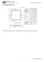
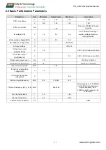
Page 10: ...IC Development Guide 10 www dwin global com DWIN Technology Professional Creditable Successful 2 2 Packaging Dimension For PCB design please refer to the DWIN official device packaging and reference d...

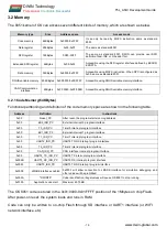
Page 11: ...0 3 AD input voltage V Vref 0 3 IO high level output amplitude VOH V 3 0 VIO 3 3V IO load current 8mA IO low level 1utput amplitude Vol V 0 3 VIO 3 3V IO load current 8mA IO high level output current...

Page 12: ...er capacitors as close as possible to the IC supply pins to reduce noise emission 4 When IO input signal is over 0 3V of VIO voltage IO must be protected by voltage divider or clamp otherwise it may c...

Page 13: ...the good real time performance fast IO rate and stable reliability of 8051 DWIN has significantly improved the 8051 memory by optimizing the code processing expanding the SFR bus and enhancing the ha...

Page 14: ...de space D_PAGESEL 0X95 0X02 32KB RAM space accessed by MOVX 0x8000 0xFFFF MUX_SEL 0XC9 0x60 orconfiguration according to application needs Peripheral multiplexing selection 7 1 CAN interface leads to...

Page 15: ...code memory space are shown in the following table Address Definition Instructions 0x00 Reset_PC After reset the program starts running address 0x00 EX0_ISR_PC External interrupt 0 program interface...

Page 16: ...execution 5 APP_RW 1 Read variable memory 0 Write variable memory 4 APP_ACK Hardware answer to 8051 request to occupy variable memory 1 OK 0 BUSY 3 0 Corresponding to DATA3 DATA0 Write enable 1 corre...

Page 17: ...MMODE 0AFH Start read mode JNB APP_ACK Waiting for confirmation MOV R0 TEST_BUF Reading demo MOV R1 2 RDVP SETB APP_EN Start reading data once JBAPP_EN MOV R0 DATA3 INC R0 MOV R0 DATA2 INC R0 MOV R0 D...

Page 18: ...DPC 0X01 After MOVX instruction operation DPTR DPTR 1 DPC 0X03 After MOVX instruction operation DPTR DPTR 1 DPH 0X83 DPTR data pointer DPL 0X82 The address space from 0x0000 to 0x7FFF prohibit using M...

Page 19: ...ditional data storage for users The following table is defined EXADR Definition Instruction 0x00 MDU_A7 Maximum bit of MDU A register 64bit 0x07 MDU_A0 Minimum bit of MDU A register 64bit 0x08 MDU_B7...

Page 20: ...MDU_A MDU_B MDU_C register group of extended SFR registers DIV_CN 0XE6 DIV hardware divider control register division C A quotient A remainder B is defined as follows 7 DIV enable Write 1 to perform...

Page 21: ...T5L_ASIC Development Guide 21 www dwin global com DWIN Technology Professional Creditable Successful MOV R6 EXDATA MOV R5 EXDATA MOV R4 EXDATA MOV R3 EXDATA MOV R2 EXDATA MOV R1 EXDATA MOV R0 EXDATA...

Page 22: ...election 0 CPU main frequency 12 1 CPU mainfrequency 24 6 4 must write 1 3 1 must write 0 0 TR2 1 T2 run 0 T2 close TH2 0xCD T2 running value automatically loaded every time counting overflow TH2 CRCH...

Page 23: ...to the main frequency of CPU 206 4384 MHz T2 1mS interruption is set to output 500 MHz square wave at P 1 0 ORG 002BH T2 interrupt program entry LJMP T21NT T21NT CLR TF2 T2 interrupt program CPL P1 0...

Page 24: ...ed with a software watchdog WDT timer whose counting reset time is set to 1 second corresponding to 11 0592 MHz crystal Once the WDT is turned on the software needs to feed the dog in the counting res...

Page 25: ...gh IT0 and IT1 In addition to the need to control the output switch output strength and peripheral multiplexing power on initialization configuration the subsequent use of IO is consistent with the st...

Page 26: ...me The WDT count becomes zero and the watchdog s overflowing time is 1 PORTDRV 0xF9 Driver capability configuration of IO port output mode 0x00 4mA 0x01 8mA recommended values 0x02 16mA 0x03 32mA The...

Page 27: ...d rate generator selection 0x00 T1 timer standard 8051 0x80 SRELOH L PCON 0x87 7 SMOD baud rate frequency doubling selection 0 no frequency doubling 1 frequency doubling SRELOH 0xBA When ADCON 0x80 SR...

Page 28: ...it 4 REN 3 TB8 2 RB8 1 TI 0 RI Clearing the SCON1 bit mark requires two consecutive writings such as ANL SCON1 0FEH ANL SCON1 0FEH SBUF1 0x9C UART3 transceiver data interface SREL1H 0xBB UART3 baud ra...

Page 29: ...t received in 9bit mode 4 1 Write 0 0 R RI receive mark Set when the stop bit is received when a valid stop bit is received SBUF2_TX 0x9E UART4 sending data interface SBUF3_RX 0x9F UART4 receiving dat...

Page 30: ...t received in 9bit mode 4 1 Write 0 0 R RI receive mark Set when the stop bit is received when a valid stop bit is received SBUF3_TX 0xAC UART5 sending data interface SBUF4_RX 0xAD UART5 receiving dat...

Page 31: ...n no longer update the data 5 CAN_RX_IF CAN sending interrupt mark and clear after hardware placement 4 OI receiving overflow markers hardware blanking software clearance is required 3 EI error mark C...

Page 32: ...h 5 bit 0xFF 0066 D3 D0 4 Data Send data DATA1 DATA4 0xFF 0067 D3 D0 4 Data Send data DATA5 DATA8 0xFF 0068 D3 1 CAN_RX_B UFFER 7 IDE 6 RTR 3 0 DLC frame data length D2 D0 3 Undefined 0xFF 0069 ID ID...

Page 33: ...control bit 2 EX1 external interrupt 1 P3 1 pin interrupt enabling control bit 1 ET0 T0 timer interrupt enable control bit 0 EX0 external interrupt 1 P3 0 pin interrupt enabling control bit IEN1 0xB8...

Page 34: ...r interrupt UART5 receive interrupt 2 There are four levels of priority among the six groups which can be configured by the corresponding bits of IP0 and IP1 according to the table below Inter group p...

Page 35: ...150 instructions on average and the interrupt execution time is short so the real time performance is already very high It is not recommended to use interrupt embedding that makes program architectur...

Page 36: ...1 XCH A Ri 1 2 MUL AB 1 4 XCHD A Ri 1 2 DIV AB 1 4 ACALL addr11 2 2 DA A 1 1 LCALL addr16 3 3 ANL ORL XRL A Rn 1 1 RET RETI 1 4 ANL ORL XRL A direct 2 2 AJMP addr11 2 2 ANL ORL XRL A Ri 1 2 LJMP addr...

Page 37: ...2 2 CPU main frequency crystal frequency 56 3 11 0592MHz crystal corresponds to 206 438MHz main frequency corresponding to an instruction cycle 1T of 4 844nS Example Under 11 0592 MHz crystal the fol...

Page 38: ...lation the jumper pad on the JMARK interface side is disconnected 2 The AGDI driver is installed to enable Keil to support T5 and HME05 simulators After installation select and configure according to...

Page 39: ...user s original 8051 code it can be done quickly by taking care of the following aspects 1 According to the hardware design after reset the startup A51 C51 startup code or initcpu program provided by...

Page 40: ...erface 4 The OS CPU 8051 program can be downloaded through the USB interface and automatically reset by hardware 5 Read and write DGUS variable memory and download pictures and word libraries through...

Page 41: ...stions during the use of this document or DWIN products or want to know more about the latest information of DWIN products please contact us Hotline 400 018 9008 Whatsapp 8619192113166 DWIN website ht...

Reviews: