T5L_ASIC Development Guide
- 15
-
www.dwin-global.com
DWIN Technology
Professional,
Creditable,
S
uccessful
3.2 Memory
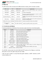
The 8051 kernel of OS can access seven different kinds of memory, which are shown as below.
Memory type
Size
Address space
Access mode
Code memory
64KBytes
0x0000-0xFFFF
It can only be read by MOVC instruction, same as standard
8051.
Data register
256Bytes
0x00-0xFF
The same as standard 8051
SFR register
128Bytes
0X80-0XFF
The same as standard 8051. DWIN can provide user SFR
definition files( .INC or .H header file).
Extended SFR register
64Bytes
0x00-0x3F
Accessible using the SFR register interface defined by EXADR,
EXDATA.
Data memory
32KBytes
0x8000-0xFFFF
Accessible using MOVX instruction. When DPC is configured as
0x00, same as standard 8051.
DGUS variable memory
256KBytes 0x00:0000-0x00:FFFF
Accessible using DGUS variable memory interface.
CAN Communication
interface
48Bytes
0xFF:0060-0xFF:006B
Accessible using DGUS variable memory interface.
3.2.1 Code Memory(64KBytes)
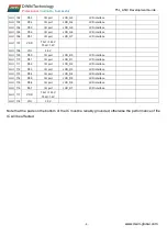
Functional partitioning and definition of the code memory space are shown in the following table.
Address
Definition
Instructions
0x00
Reset_PC
After reset, the program starts running address .
0x00
EX0_ISR_PC
External interrupt 0 program interface
0x00
T0_ISR_PC
Timer0 interrupt program interface
0x00
EX1_ISR_PC
External interrupt 1 program interface
0x00
T1_ISR_PC
Timer1 interrupt program interface
0x00
UART2_ISR_PC
UART2 TX/RX interrupt program interface
0x00
T2_ISR_PC
Timer2 interrupt program interface
0x00
CAN_ISR_PC
CAN interface interrupt program interface
0x00
UART4_TX_ISR_PC
UART4 TX interrupt program interface
0x006B
UART5_RX_ISR_PC
UART5 RX interrupt program interface
0x0083
UART3_ISR_PC
UART3 TX/RX interrupt program interface
0x00F8
JMARK interface enabled
0xFFFF will allow connection to JMARK interface for simulation debugging, and
other values will be prohibited.
0x00FA
"DWINT5"
Code identification, illegal values will cause OS 8051 to stop running.
0x0100
Application code start
Maximum 63.75KB
The OS 8051 code is stored in the 0x01:0000-0x01:FFFF position of the 1Mbytes on chip Flash.
After power-on reset, the system loads and runs in RAM.
Code can only be written to on-chip Flash through SD interface or UART1 interface (or WIFI
network interface, etc).


