Embedded Solutions
Page 15 of 37
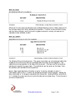
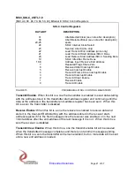
BIS3_ID
[$04] BiSerial III FLASH status/Driver Status Port read only
Design Number / FLASH Revision
DATA BIT
DESCRIPTION
31-16
Design/Driver ID
15-0
FLASH revision
FIGURE 5
PMC BISERIAL-III SDLC DESIGN ID REGISTER BIT MAP
The Design/Driver ID for the SDLC project is 0x0003. The FLASH revision is currently
0x0001, but will be updated as features are added or revisions made.
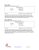
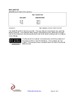
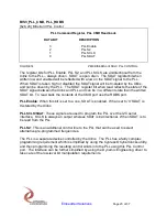
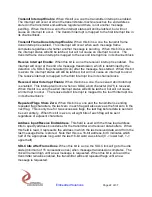
BIS3_IO_DATA
[$10] BiSerial III Parallel Data Output Register read/write
Parallel Data Output Register
DATA BIT
DESCRIPTION
31-0
parallel output data
FIGURE 6
PMC BISERIAL-III SDLC PARALLEL OUTPUT DATA BIT MAP
There are 32 potential output bits in the parallel port. The Direction, Termination, and
Mux Control registers are also involved. When the direction is set to output, and the
Mux control set to parallel port the bit definitions from this register are driven onto the
corresponding parallel port lines.
This port is direct read/write of the register. The I/O side is read-back from the
BIS3_IO_RDBK port. It is possible that the output data does not match the I/O data in
the case of the Direction bits being set to input or the Mux control set to state-machine.


