background image


Rev. 0.2 / 09 /2015 


10 

AN1111-2 

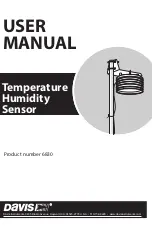
The nominal characteristic of the device (HCT01 sensor together with electronics) can be determined 

by measurement at various levels of relative humidity. 


Figure 7: Example of nominal characteristic 

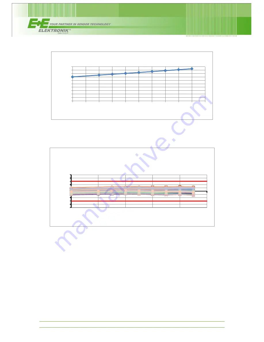
The deviation from the reference RH after correcting for PCB influences and hysteresis is shown in 
Figure 8.  


Figure 8: Initial accurate electronics – w/o C_Cal: PCB corrected 


10 

20 

30 

40 

50 

60 

70 

80 

90 

100 

10 

20 

30 

40 

50 

60 

70 

80 

90 

100 

di

gi

ta

l c

ap

ac

ita

nc

e v

al

ues

 [p

F]


relative humidity [% rH] 

Example of nominal characteristic @3V3 

-5,0 

-4,0 

-3,0 

-2,0 

-1,0 

0,0 

1,0 

2,0 

3,0 

4,0 

5,0 

20 

40 

60 

80 

100 

de

vi

at

io

re

la

tiv

hu

mi

di

ty

 [%  rH

relative humidity [% rH] 

Initial accurate electronics, 55 units @3V3 

w/o  C_CAL ; PCB corrected ;  w/o hysteresis; nominal 

characeristic 

Summary of Contents for HCT01

Page 1: ...Rev 0 2 09 2015 2 AN1111 2 Developer s Guide for HCT01 Humidity and Temperature Sensors...

Page 2: ...2 1 Schematic circuit diagram 6 2 1 1 Bill of Material 6 2 1 2 Correlation between sensor capacity and period 7 3 RH measurement with pre adjusted HCT01 and microcontroller based initially accurate c...

Page 3: ...gives an overview on the accuracy which can be achieved by various combinations of HCT01 circuitry Using an unadjusted RH sensor HCT01 00 implies humidity calibration for the device built with it The...

Page 4: ...Rev 0 2 09 2015 5 AN1111 2 Choice of HCT01 version and driving circuitry Figure 1 Circuitry options for HCT01...

Page 5: ...ive humidity at the sensor The accurate measurement of the period requires a precise time base such as a quartz crystal 2 1 Schematic circuit diagram Figure 2 Circuitry with frequency output 2 1 1 Bil...

Page 6: ...n 95 pF 25 4 s cycle duration Figure 3 The sensitivity is approx 0 064 s rH with a rise of 0 25 pF rH Figure 4 Nominal characteristic of the measuring device with frequency output Figure 5 Example of...

Page 7: ...ailable in the E E patent EP 1 574 847 B1 US 7 084 644 B2 3 1 Schematic circuit diagram Figure 6 Schematic circuit design 1 There are three possible measurement paths 1 Sensor capacitance path with R1...

Page 8: ...parator reaches the voltage at the voltage divider no repeat point 2 and recharge the reference yes end of loop and save the numbers of charge discharge events 6 Each cycle measures the reference path...

Page 9: ...B influences and hysteresis is shown in Figure 8 Figure 8 Initial accurate electronics w o C_Cal PCB corrected 0 10 20 30 40 50 60 70 80 90 100 0 10 20 30 40 50 60 70 80 90 100 digital capacitance val...

Page 10: ...l test and layout optimizing loops These imply tests for assessing the impact of the stay capacitance and its variations on the output signal of the device as follows 1 Test a sample of relevant size...

Page 11: ...0 Fax 43 7235 605 8 E Mail info epluse com Homepage www epluse com Please visit our website to find your local contact 6 Revision history Date Revision number Changes November 2011 V_0 1 Initial relea...

Reviews: