Chengdu Ebyte Electronic Technology Co., Ltd.
User Manual
Copyright ©2012–2021
,
Chengdu Ebyte Electronic Technology Co., Ltd.
6
3
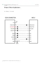
MISO_TX
Output
SPI data output pin; can also be used as UART transmit pin (see SX1280 manual
for details)
4
MOSI_RX
Input
SPI data input pin; can also be used as a UART receive pin (see SX1280 manual
for details)
5
SCK_RTSN
Input
SPI clock input pin; can also be used as a UART request to transmit pin
(see SX1280 manual for details)
6
NSS_CTS
Input
Module chip select pin, used to start an SPI communication; also used for
UART clear transmit pin (See SX1280 manual for details)
7
GND
Ground wire, connected to the power reference ground
8
RX_EN
Input
LNA control pin, active high
9
TX_EN
Input
PA control pin, active high
10
GND
Ground wire, connected to the power reference ground
11
NRESET
Input
Chip reset trigger input pin, active low, built-in pull-up resistor 50K
12
BUSY
Output
Used for status indication (see SX1280 manual for details)
13
DIO1
Input/Output
Configurable general-purpose IO ports (see SX1280 manual for details)
14
DIO2
Input/Output
Configurable general-purpose IO ports (see SX1280 manual for details)
15
DIO3
Input/Output
Configurable general-purpose IO ports (see SX1280 manual for details)
16
GND
Ground wire, connected to the power reference ground
Chapter 4 Basic Operations
4.1
Hardware design
It is recommended to use a DC regulated power supply to supply power to the module, the power supply
ripple coefficient should be as small as possible, and the module should be grounded reliably;
Please pay attention to the correct connection of the positive and negative poles of the power supply,
such as reverse connection may cause permanent damage to the module;
Please check the power supply to ensure that it is between the recommended power supply voltages.
If it exceeds the maximum value, the module will be permanently damaged;
Please check the stability of the power supply, the voltage should not fluctuate greatly and
frequently;
When designing the power supply circuit for the module, it is often recommended to reserve more than
30% of the margin, so that the whole machine can work stably for a long time;
The module should be kept as far away as possible from the power supply, transformer, high-frequency
wiring and other parts with large electromagnetic interference;
High-frequency digital traces, high-frequency analog traces, and power traces must avoid the
underside of the module. If it is absolutely necessary to pass under the module, assuming that the
module is soldered on the Top Layer, lay copper on the Top Layer of the contact part of the module.
Copper and well grounded), must be close to the digital part of the module and routed on the Bottom
Layer;


