background image

Chengdu Ebyte Electronic Technology Co,;Ltd

E70-433T14S user manual

Copyright ©2012–2019

Chengdu Ebyte Electronic Technology Co,;Ltd

23

9.1 Download Program

Key word

Notes

Input program

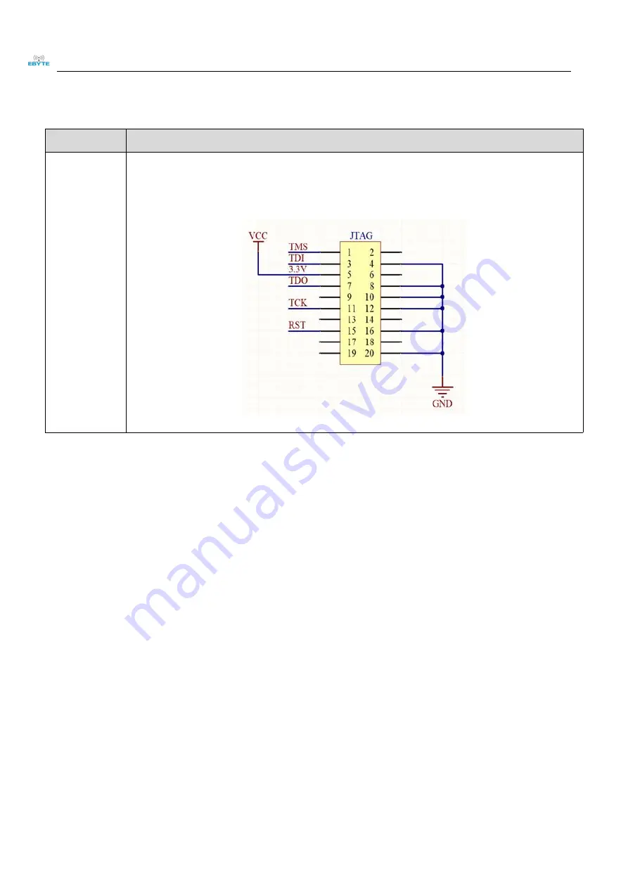
The module is SOC with GPIO port. For program downloading, please use the special downloader of CC series:

JTAG (or the original CC1310 board from TI), any other serial port or ISP, ICP are unavailable to download. Below

is the connection diagram of JTAG

XDS100

. See more details in TI official document.

TDI and TDO pin can be

unconnected

Connection diagram of JTAG downloader

10. Hardware design

It is recommended to use a DC stabilized power supply. The power supply ripple factor is as small as possible, and
the module needs to be reliably grounded.

Please pay attention to the correct connection of the positive and negative poles of the power supply. Reverse
connection may cause permanent damage to the module

Please check the power supply to ensure it is within the recommended voltage otherwise when it exceeds the
maximum value the module will be permanently damaged

Please check the stability of the power supply, the voltage can not be fluctuated frequently

When designing the power supply circuit for the module, it is often recommended to reserve more than 30% of the
margin, so the whole machine is beneficial for long-term stable operation.

The module should be as far away as possible from the power supply, transformers, high-frequency wiring and other
parts with large electromagnetic interference.

High-frequency digital routing, high-frequency analog routing, and power routing must be avoided under the
module. If it is necessary to pass through the module, assume that the module is soldered to the Top Layer, and the
copper is spread on the Top Layer of the module contact part(well grounded), it must be close to the digital part of
the module and routed in the Bottom Layer

Assuming the module is soldered or placed over the Top Layer, it is wrong to randomly route over the Bottom Layer
or other layers, which will affect the module's spurs and receiving sensitivity to varying degrees

It is assumed that there are devices with large electromagnetic interference around the module that will greatly

Summary of Contents for E70-868T14S

Page 1: ...E70 868T14S User Manuel CC1310 868MHz SMD Wireless Module ...

Page 2: ...1 6 1 MODE SWITCH 12 6 2 RSSI MODE MODE 0 13 6 3 CONTINUOUS MODE MODE 1 13 6 4 SUB PACKAGE MODE MODE 2 14 6 5 CONFIGURATION MODE MODE 3 14 6 6 WAKE UP MODE MODE 4 15 6 7 CONFIGURATION MODE MODE 5 15 6 8 POWER SAVING MODE MODE 6 15 6 9 SLEEP MODE MODE 7 16 7 INSTRUCTION FORMAT 16 7 1 DEFAULT PARAMETER 17 7 2 READING OPERATING PARAMETERS 17 7 3 READING VERSION NUMBER 17 7 4 RESET INSTRUCTION 17 7 5 ...

Page 3: ...c Technology Co Ltd E70 433T14S user manual Copyright 2012 2019 Chengdu Ebyte Electronic Technology Co Ltd 2 14 ANTENNA GUIDANCE 27 14 1 ANTENNA RECOMMENDATION 27 15 PACKAGE FOR BATCH ORDER 27 REVISION HISTORY 28 ABOUT US 28 ...

Page 4: ...in low power multifunctional wireless serial program users can also according to the need for secondary development 1 2 Features Communication distance tested is up to 1 5km Maximum transmission power of 25mW software multi level adjustable Support the global license free ISM 433MHz band Support air date rate of 2 5kbps 168kbps Low power consumption for battery supplied applications Can achieve up...

Page 5: ...formance Remark Min Typ Max Operating voltage V 2 2 3 3 3 8 3 3 V ensures output power Communication level V 3 3 For 5V TTL it may be at risk of burning down Operating temperature 40 85 Industrial design Operating frequency MHz 861 876 5 Support ISM band Power consumption Transmitting current mA 27 Instant power consumption Receiving current mA 8 Turn off current μA 1 Software is shut down Max Tx ...

Page 6: ...T14S user manual Copyright 2012 2019 Chengdu Ebyte Electronic Technology Co Ltd 5 Buffer 2048Byte Modulation GFSK Communication interface UART Package SMD Connector 1 27mm Size 16 26mm Antenna IPX Stamp hole 50 ohm impedance 3 Dimension Pin definition ...

Page 7: ...Input M2 M1 M0 jointly decide the 8 working modes An external 1k protective resistor shall be connected in series and a 1M pull up resistor shall be added when in use Cannot be floated it can be grounded when not used 18 M0 Input M2 M1 M0 jointly decide the 8 working modes An external 1k protective resistor shall be connected in series and a 1M pull up resistor shall be added when in use Cannot be...

Page 8: ...eserved pin Reserved to be floated 31 NC Reserved pin Reserved to be floated 32 RESET Input Reset pin 33 NC Reserved pin Reserved to be floated 34 NC Reserved pin Reserved to be floated 35 NC Reserved pin Reserved to be floated 36 NC Reserved pin Reserved to be floated 37 NC Reserved pin Reserved to be floated 38 NC Reserved pin Reserved to be floated 39 NC Reserved pin Reserved to be floated 40 N...

Page 9: ...2019 Chengdu Ebyte Electronic Technology Co Ltd 8 4 Connect to MCU No Description STM8L MCU 1 The UART module is TTL level please collect with MCU 2 For some MCU works at 5VDC it may need to add 4 10K pull up resistor for the TXD AUX pin 5 Function description 5 1 Fixed transmission ...

Page 10: ... A as 0xFFFF or 0x0000 and the channel as 0x04 When module is the transmitter transparent transmission all modules under channel 0x04 will receive the data the purpose of broadcast is realized 5 4 Monitor address For example Set the address of module A as 0xFFFF or 0x0000 and the channel as 0x04 When module A is the receiver it can receive the data sent from all modules under channel 0x04 the purp...

Page 11: ... that are not sent yet via wireless way or whether all wireless data has been sent through UART or whether the module is still in the process of self check initialization 5 6 1 Indication of UART output To wake up external MCU 5 6 2 Indication of wireless transmitting Buffer empty the internal 1024 bytes data in the buffer are written to the RFIC Auto sub packaging When AUX 1 the user can input da...

Page 12: ...3 Configuration procedure of module Only happened when power on resetting or exiting sleep mode 6 Operating Mode The table below shows the status of corresponding modes Mode 0 7 M2 M1 M0 Mode introduction Remark 0 RSSI mode 0 0 0 UART opens Wireless closes and transmission is unavailable Module outputs RSSI value each 100ms through UART ...

Page 13: ...eve low power consumption receiving 7 Sleep mode 1 1 1 UART closes wireless transmitting is available and sleep mode is on It can be woken up by any falling edge of M2 M1 M0 6 1 Mode Switch The user can decide the operating mode by the combination of M0 M1 and M2 The two GPIOs of MCU can be used to switch mode After modifying M0 M1 or M2 it will start to work in new mode 1ms later if the module is...

Page 14: ...ry flexible and efficient It is totally designed on the basis of the user MCU s convenience at the same time the work load and power consumption of the whole system has been reduced and the efficiency of whole system is largely improved 6 2 RSSI Mode Mode 0 Status M0 1 M1 0 M2 0 Transmitting Wireless data transmission is not available Receiving Wireless data receiving is not available Baud rate ai...

Page 15: ...g Wireless data transmission is available Receiving Wireless data receiving is available Baud rate air data rate Under this mode the baud rate and air data rate are independent both receiver and transmitter can have different baud rate but same air data rate Advantage Very low air data rate can be configured for longer distance the data continuousness between output data depends on the data packet...

Page 16: ...will be added automatically before transmitting the code number depends on the wake up time Disadvantage The transmission time is long only applicable to wake up the receiver not applicable for common data transmission Applications For waking up the receiver under WOR mode Note Under wake up mode the single data packet length is 84 bytes excluding the address and channel for directional transmissi...

Page 17: ...nsmitter under mode 4 6 9 Sleep Mode Mode 7 Status M0 1 M1 1 M2 1 Transmitting Transmitting is not available Receiving Receiving is not available Others Other functions of the module are closed only can quit sleep mode by switching the M0 M1 and M2 status 7 Instruction Format In configuration mode Mode 3 M0 1 M1 1 M2 0 it supports instructions below Only support 9600 and 8N1 format when setting No...

Page 18: ... XX4 XX5 70 here means the module model E70 series xx1 is the version number and XX2 XX3 XX4 XX5 refers to the other module features 7 4 Reset Instruction Instruction format Description C4 C4 C4 In configuration mode M0 1 M1 1 M2 0 User gives the module instruction HEX format C4 C4 C4 the module resets for one time During the reset process the module will conduct self check AUX outputs low level A...

Page 19: ...ation parties 0 0 0 2 5kbps 0 0 1 5kbps 0 1 0 12kbps Default 0 1 1 28kbps 1 0 0 64kbps 1 0 1 168kbps 1 1 0 168kbps 1 1 1 168kbps 4 CHAN 7 6 5 Packet length only for sub package mode Under continuous transmitting mode M0 1 M1 0 M2 0 this parameter is invalid 0 0 0 16 bytes 0 0 1 32 bytes 0 1 0 64 bytes Default 0 1 1 128 bytes 1 0 0 256 bytes 1 0 1 512 bytes 1 1 0 1024 bytes 1 1 1 2048 bytes Communi...

Page 20: ...urn on FEC Default 2 IO drive mode This bit is used to the internal pull up resistor It also increases the level s adaptability in case of open drain But in some cases it may need external pull up resistor 0 TXD and AUX push pull outputs RXD pull up inputs 1 TXD AUX open collector outputs RXD open collector inputs 1 0 transmission power approximation The external power must ensure that the ability...

Page 21: ...2019 Chengdu Ebyte Electronic Technology Co Ltd 20 9 Secondary Development E70 series have built in CC1310 SoC chip Users can conduct the development according to pin description below Meanwhile Ebyte can develop the customized software for customers Please contact us for more detail ...

Page 22: ...trode 2 ANT Antenna 50Ω characteristic impedance 3 X32K_Q1 Input Output Connect to 32 768K quartz crystal with pin 4 4 X32K_Q2 Input Output Connect to 32 768K quartz crystal with pin 3 5 DIO_1 Input Output MCU GPIO 6 DIO_2 Input Output MCU GPIO 7 DIO_3 Input Output MCU GPIO 8 DIO_4 Input Output MCU GPIO 9 DIO_5 Input Output MCU GPIO 10 DIO_6 Input Output MCU GPIO 11 DIO_7 Input Output MCU GPIO 12 ...

Page 23: ...TCKC Input JTAG TCKC 23 DIO_16 Input Output MCU GPIO 24 DIO_17 Input Output MCU GPIO 25 DIO_18 Input Output MCU GPIO 26 VCC Positive power reference voltage range 2 2V 3 8V DC 28 DIO_19 Input Output MCU GPIO 29 DIO_20 Input Output MCU GPIO 30 DIO_21 Input Output MCU GPIO 31 DIO_22 Input Output MCU GPIO 32 RESET Input Reset pin 33 DIO_23 Input Output MCU GPIO 34 DIO_24 Input Output MCU GPIO 35 DIO_...

Page 24: ... the maximum value the module will be permanently damaged Please check the stability of the power supply the voltage can not be fluctuated frequently When designing the power supply circuit for the module it is often recommended to reserve more than 30 of the margin so the whole machine is beneficial for long term stable operation The module should be as far away as possible from the power supply ...

Page 25: ...led inside the metal case which will cause the transmission distance to be greatly weakened 11 FAQ 11 1 Communication range is too short The communication distance will be affected when obstacle exists Data lose rate will be affected by temperature humidity and co channel interference The ground will absorb and reflect wireless radio wave so the performance will be poor when testing near ground Se...

Page 26: ...uality are poor or too long so the bit error rate is high 12 Production guidance 12 1 Reflow soldering temperature Profile Feature Sn Pb Assembly Pb Free Assembly Solder Paste Sn63 Pb37 Sn96 5 Ag3 Cu0 5 Preheat Temperature min Tsmin 100 150 Preheat temperature max Tsmax 150 200 Preheat Time Tsmin to Tsmax ts 60 120 sec 60 120 sec Average ramp up rate Tsmax to Tp 3 second max 3 second max Liquidous...

Page 27: ...T14S2 CC1310 915M 14 1 5 2 5k 168k DIP 14 20 IPEX Stamp hole E70 433T14S2 CC1310 433M 14 1 5 2 5k 168k DIP 14 20 IPEX Stamp hole E70 915T14S CC1310 915M 14 1 5 2 5k 168k DIP 16 26 IPEX Stamp hole E70 868T14S CC1310 868M 14 1 5 2 5k 168k DIP 16 26 IPEX Stamp hole E70 915T30S CC1310 915M 30 6 2 5k 168k DIP 24 38 5 IPEX Stamp hole E70 868T30S CC1310 868M 30 6 2 5k 168k DIP 24 38 5 IPEX Stamp hole E70...

Page 28: ...y improve the communication system Therefore we recommend some antennas for wireless modules with excellent performance and reasonable price Model No Type Frequency Hz Interface Gain dBi Height Cable Function feature TX868 XP 100 Sucker Antenna 4868M SMA J 3 5 29cm 100cm Sucker antenna High gain TX868 JK 20 Rubber antenna 868M SMA J 3 200mm Flexible omnidirectional TX868 JZ 5 Rubber antenna 868M S...

Page 29: ...ting huaa 1 20 2018 05 24 content updating Huaa 1 21 2018 07 20 name change Huaa 1 30 2018 10 29 module separating Huaa 1 4 2019 12 06 Ren About us Technical support support cdebyte com Documents and RF Setting download link www ebyte com Thank you for using Ebyte products Please contact us with any questions or suggestions info cdebyte com Fax 028 64146160 ext 821 Web www ebyte com Address Innova...

Page 30: ...Chengdu Ebyte Electronic Technology Co Ltd E70 433T14S user manual Copyright 2012 2019 Chengdu Ebyte Electronic Technology Co Ltd 29 ...

Reviews: