background image

Hardware Reference Manual


SOM 


Version 1.0 

 - 40 - 

eInfochips Confidential 


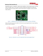
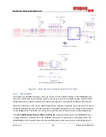
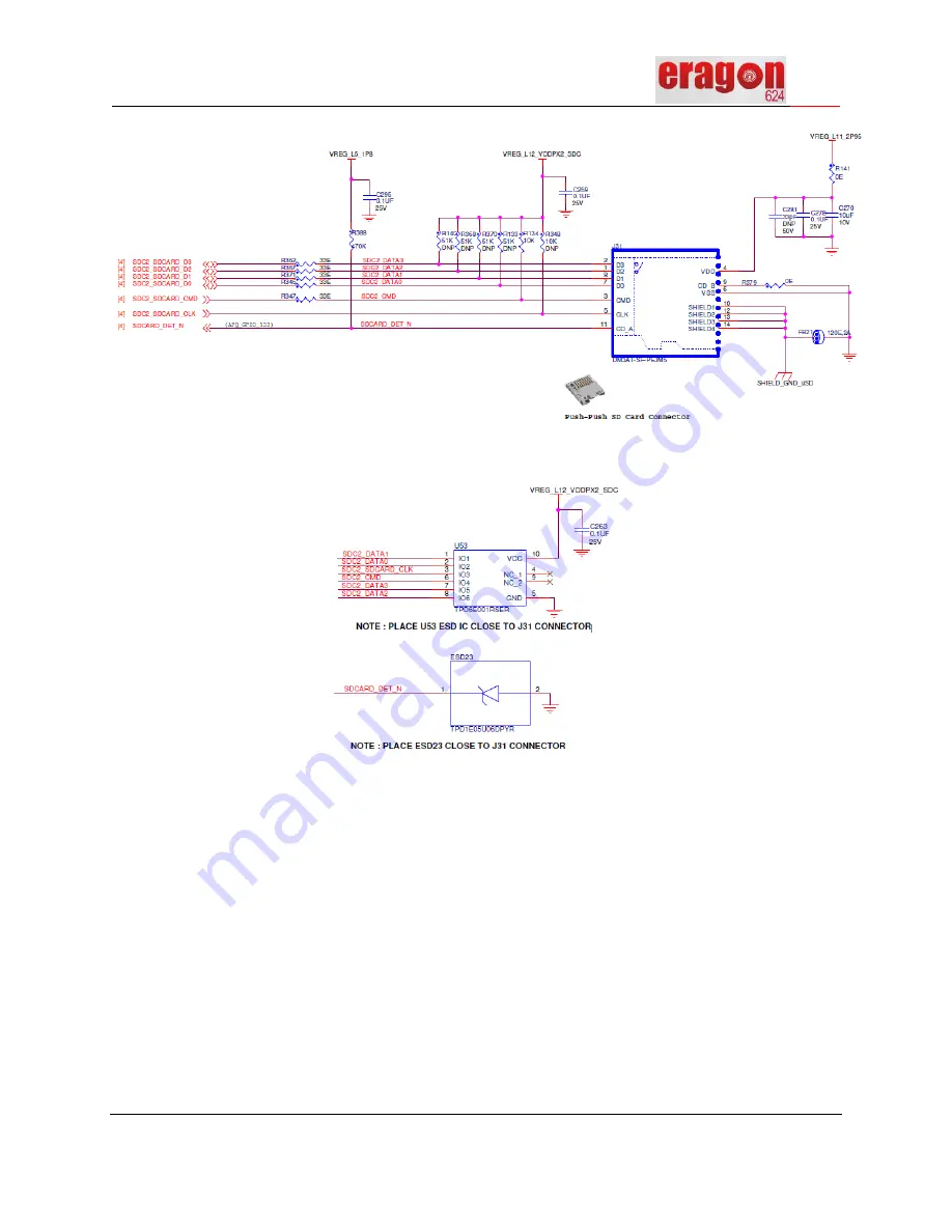
Figure 13 – Micro SD card connector schematic for carrier


6.3.8


DSI to HDMI 

The Qualcomm APQ8053 Processor does not include a built-in HDMI interface. The ERAGON624 has 
the built-in MIPI-DSI 4 lanes interface, which is used, as a source for the HDMI output. A DSI to HDMI 
Bridge Board can be used to performs this task and it supports a resolution from 480p to 720p at 30Hz. 


While  the  ADV7533  on  the  DSI  to  HDMI  Bridge  board  supports  automatic  input  video  format  timing 
detection (CEA-861E) and an I2C channel from the APQ8053 allows the user to configure the operation 
of this Bridge Board. The BLSP3_I2C interface is used from the SoC that connects to the Bridge board. 


This DSI to HDMI Bridge Board (eI PN# 17_00278_02) supports audio as well. The ERAGON624 uses 
a  single  bit  MI2S_1  interface  from the  APQ8053  chip  which  is mentioned  in  the  below  block.  The 
ERAGON624 carrier should contains the 14 pin HDMI Audio Connector to connect to the Bridge Board. 

Summary of Contents for Eragon 624 SOM

Page 1: ......

Page 2: ...hips intellectual property including the copyrights in all countries in the world This document is provided under a license to use only with all other rights including ownership rights being retained...

Page 3: ...ites 16 Starting the Eragon624 SOM for the first time with Eragon624 Carrier 16 6 System Block Diagram 17 ERAGON624 BOARD IMAGE 18 Major Blocks of ERAGON624 SOM Module 31 6 2 1 Processor APQ8053 Featu...

Page 4: ...BT chip antenna 42 6 3 11 GPS chip antenna 43 6 3 12 M 2 4G LTE connector 43 6 3 13 RTC 47 6 3 14 Debug Port 47 7 Electrical Specification 48 Absolute Maximum Ratings 48 Operating Conditions 48 8 Mech...

Page 5: ...Carrier Board for Audio Code Daughter Board 37 Figure 10 Audio Headset Jack 37 Figure 11 Audio Headset Jack schematic 37 Figure 12 Analog and Digital Codec Headers J17 J18 38 Figure 13 Micro SD card...

Page 6: ...34 Table 5 Headset J19 Pinout 38 Table 6 Audio Header J17 Pinout 39 Table 7 Audio Header J18 Pinout 39 Table 8 HDMI Audio Connector J26 Pinout 41 Table 9 HDMI Audio Connector J27 Pinout 42 Table 10 M...

Page 7: ...9 eInfochi ps Initial release Table 1 Document History 1 2 Definition Acronyms and Abbreviations Definition Acronym Abbreviation Description BLE Bluetooth Low Energy BOM Bill of Material BT Bluetooth...

Page 8: ...Kilo Byte LAN Local Area Network LPDDR Lower Power DDR MIPI Mobile protocol working Alliance not an Acronym MISO Master In Slave Out MMC Multi Media Card MOSI Master Out Slave In MP Mega Pixel OTG On...

Page 9: ...eference Manual SOM Version 1 0 9 eInfochips Confidential UART Universal Asynchronous Interface USB Universal Serial Bus ADB Android Debug Bridge WLAN Wireless LAN Table 2 Definition Acronyms and Abbr...

Page 10: ...rdware Reference Manual SOM Version 1 0 10 eInfochips Confidential 1 3 References No Document Version Remarks 1 ERAGON624 SOM Schematic File 1 3 2 ERAGON624 Carrier Schematic File 1 3 Table 3 Referenc...

Page 11: ...port of your permitted use of the ERAGON624 development platform under the Agreement Distribution of this document is strictly prohibited without the express written permission of eInfochips Ltd and i...

Page 12: ...tended Audience This document is intended for technically qualified personnel It is not intended for general audiences Intended Use The development platform supports a wide range of industry interface...

Page 13: ...re CPU high performance Adreno 506 GPU and a dedicated DSP for advanced A V processing The SOM is equipped with full range of interfaces available in the Qualcomm Snapdragon APQ8053 SoC which are rout...

Page 14: ...PMIC Codec o 1x Earphone output PMIC Codec o 1x Lineout PMIC Codec Memory RAM Up to 4GB LPDDR3 at up to 933 MHz clock Storage Up to 64 GB eMMC Connectivity WLAN 802 11 b g n 2 4GHz and 802 11 a n ac...

Page 15: ...ent target markets Some of the typical applications are Consumer Electronics Internet of Things Marine Automotive Domestic Robot Digital signage Security Surveillance Biometric Access Control Systems...

Page 16: ...sion is given FFC Cable for connecting LCD display to the ERAGON 624 Board Starting the Eragon624 SOM for the first time with Eragon624 Carrier To start the board follow these simple steps Step 1 Firs...

Page 17: ...Hardware Reference Manual SOM Version 1 0 17 eInfochips Confidential 6 System Block Diagram Figure 1 ERAGON 624 SOM Block Diagram...

Page 18: ...Hardware Reference Manual SOM Version 1 0 18 eInfochips Confidential ERAGON624 BOARD IMAGE Figure 2 ERAGON624 SOM Top View Figure 3 ERAGON624 SOM BOT View...

Page 19: ...6 J11 6 CSI2_CAM_GPIO_1 CSI2 Camera GPIO 1 8V J5 7 J11 7 CSI0_RST CSI0 Camera Reset Signal 1 8V J5 8 J11 8 CSI2_CAM_GPIO_2 CSI2 Camera GPIO 1 8V J5 9 J11 9 CSI2_PWDN CSI2 Camera Power Down signal 1 8V...

Page 20: ...34 J11 34 GND Ground J5 35 J11 35 MIPI_CSI1_LANE2_N MIPI CSI1 Lane 2 Negative J5 36 J11 36 MIPI_CSI2_LANE3_P MIPI CSI2 Lane 3 Positive J5 37 J11 37 GND Ground J5 38 J11 38 MIPI_CSI2_LANE3_N MIPI CSI2...

Page 21: ...I CSI0 Lane1 Negative J5 60 J11 60 MIPI_DSI1_LANE2_N MIPI DSI1 Lane2 Negative J5 61 J11 61 GND Ground J5 62 J11 62 MIPI_DSI1_LANE2_P MIPI DSI1 Lane2 Positive J5 63 J11 63 MIPI_CSI0_LANE2_P MIPI CSI0 L...

Page 22: ...84 J11 84 MIPI_DSI0_LANE1_P MIPI DSI0 Lane1 Positive J5 85 J11 85 CSI_I2C0_SDA CCI0 Camera I2C Data Signal 1 8V J586 J11 86 MIPI_DSI0_LANE1_N MIPI DSI0 Lane1 Negative J5 87 J11 87 CAM_MCLK2 24Mhz Mast...

Page 23: ...4V Input voltage 3 8 J4805 9 J13 9 VBAT 3 5V 4 4V Input voltage 3 8 J4805 10 J13 10 VBAT 3 5V 4 4V Input voltage 3 8 J4805 11 J13 11 VBAT 3 5V 4 4V Input voltage 3 8 J4805 12 J13 12 VBAT 3 5V 4 4V In...

Page 24: ...tery Thermistor 2 7 J4805 35 J13 35 PMI_CHG_EN PMI Charge Enable control signal J4805 36 J13 36 BAT_THERM PMI Battery Thermistor signal J4805 37 J13 37 GND Ground J4805 38 J13 38 BAT_CON_ID PMI Batter...

Page 25: ...sense 5 J4805 60 J13 60 PMC_HPH_REF PMIC Headphone reference J4805 61 J13 61 LCD_BL_LED_K1 Display backlight LED cathode 1 J4805 62 J13 62 PMIC_HPH_L PMIC Headphone left channel J4805 63 J13 63 LCD_BL...

Page 26: ...86 J13 86 PMIC_MIC_BIAS2 PMIC MIC Bias 2 voltage out J4805 87 J13 87 VREG_L2_1P1 PMIC LDO2 output voltage 1 2 J4805 88 J13 88 EXT_RF_CLK3 19 2 MHz RF clock 3 J4805 89 J13 89 USB_VCONN USB Type C Vconn...

Page 27: ...ontrol 1 8 J4804 10 J16 10 GND Ground J4804 11 J16 11 GND Ground J4804 12 J16 12 BLSP1_SPI_MOSI BLSP1 SPI MOSI 1 8 J4804 13 J16 13 SDC2_SDCARD_D3 SDC2 SDCARD Data 3 1 8 2 95 J4804 14 J16 14 BLSP1_SPI_...

Page 28: ...35 TP_I2C_SCL Display I2C clock 1 8 J4804 36 J16 36 SPKR_AMP_EN1 Speaker amplifier Enable 1 1 8 J4804 37 J16 37 TP_I2C_SDA Display I2C data 1 8 J4804 38 J16 38 UART_MSM_TX BLSP2 UART transmit Debug UA...

Page 29: ...round J4804 60 J16 60 BLSP4_UART_RX BLSP4 UART receive 1 8 J4804 61 J16 61 WDOG_DISABLE Watchdog disable 1 8 J4804 62 J16 62 BLSP4_I2C_SDA BLSP4 I2C Data 1 8 J4804 63 J16 63 USB_HUB_RST_N USB HUB rese...

Page 30: ...O87 HDMI Interrupt 1 8 J4804 84 J16 84 BLSP8_SPI_CLK BLSP8 SPI clock 1 8 J4804 85 J16 85 PMI_WLED_EN_N PMI White LED Enable J4804 86 J16 86 BLSP8_SPI_MOSI BLSP8 SPI MOSI 1 8 J4804 87 J16 87 GND Ground...

Page 31: ...l storage devices interfaced through SDC2 Multimedia features Supports Three 4 Lane CSI Ports at 2 1 Gbps per lane data rate however only two can work concurrently as it has only two ISPs All three MI...

Page 32: ...ution that integrates two different wireless connectivity technologies into a single device the interfaces are Dual band 2 4GHz and 5GHz WLAN compliant with IEEE 802 11 a b g n specifications and supp...

Page 33: ...s There are three notification LEDs provided on SOM module as described below LED2 APQ reset out LED It s glow indicates that processor came out of reset and booted successfully LED3 Charging LED Indi...

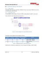
Page 34: ...t modes placing the switch on carrier card Below schematic can be followed for Boot configuration Figure 4 Boot Configuration Switch SW1 schematic Below table mentions different boot configurations op...

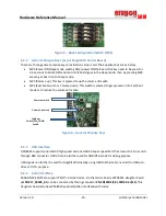
Page 35: ...ch is pressed to get processor into Fast boot mode or to reduce the volume of media Figure 6 General Purpose Keys 6 3 4 USB Interface APQ8053 supports one USB2 0 high speed and one USB3 0 Super speed...

Page 36: ...peripherals excluding can be connected on headset connector J19 Female headers J17 J18 These Provisions can be given to carrier board for Audio interfaces Figure 7 WCD9335 Audio Code Daughter Board cu...

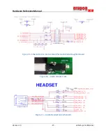
Page 37: ...rdware Reference Manual SOM Version 1 0 37 eInfochips Confidential Figure 9 Schematic 2 on Carrier Board for Audio Code Daughter Board Figure 10 Audio Headset Jack Figure 11 Audio Headset Jack schemat...

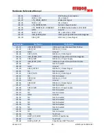
Page 38: ...igital Codec Headers J17 J18 Below is the Pinout Specification of J17 Pin Number Net Name Pin Function J17 1 CONN_CDC_MIC1_P MIC1 Input Positive J17 2 CONN_CDC_MIC5_P MIC5 Input Positive J17 3 GND Gro...

Page 39: ...gital MIC_2 Data J18 13 CDC_LINE_OUT2_P Line Output_2 Positive J18 14 CDC_LINE_OUT1_P Line Output_1 Positive J18 15 CDC_LINE_OUT2_M Line Output_2 Negative J18 16 CDC_LINE_OUT1_M Line Output_1 Negative...

Page 40: ...ution from 480p to 720p at 30Hz While the ADV7533 on the DSI to HDMI Bridge board supports automatic input video format timing detection CEA 861E and an I2C channel from the APQ8053 allows the user to...

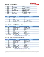
Page 41: ...y J26 11 NC Not Connected J26 12 VCC_5V0 5V Supply J26 13 NC Not Connected J26 14 VCC_3V3 3 3V Supply Table 8 HDMI Audio Connector J26 Pinout 6 3 9 HDMI to CSI Audio interface The Qualcomm APQ8053 Pro...

Page 42: ..._1_D1 I2S Data 1 Signal J27 12 MI2S_1_D0 I2S Data 0 Signal J27 13 HDMI_INT_GPIO HDMI Interrupt J27 14 HDMI_RST_N HDMI Reset J27 15 GND Ground J27 16 GND Ground Table 9 HDMI Audio Connector J27 Pinout...

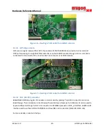
Page 43: ...onnector J21 at Carrier Card to connector J1 at SOM module Figure 17 Routing of UFL cable from SOM to Carrier 6 3 12 M 2 4G LTE connector ERAGON624 SOM to plug 4G LTE modem on Carrier card by placing...

Page 44: ...pply For LTE Modem J35 5 GND Ground J35 6 LTE_MODEM_POWER LTE Modem Power Control Signal J35 7 USBDN_DP2 USB High Speed Data Positive Signal J35 8 LTE_MODEM_W_DISABLE 1 LTE RF Radio Disable control GP...

Page 45: ...35 35 USB_SSTXM_DN2 USB Super Speed Transmit Data Negative J35 36 SIM1_PWR SIM Card _1 Power Supply J35 37 USB_SSTXP_DN2 USB Super Speed Transmit Data Positive J35 38 NC Not Connected J35 39 GND Groun...

Page 46: ...r J35 Pinout SIM Card_1 Connector Pin specifications are as follows Pin Number Net Name Pin Function J38 1 SIM1_PWR_SOCKET SIM1 Power Supply J38 2 SIM1_RST_ESD SIM1 Reset Signal J38 3 SIM1_CLK_ESD SIM...

Page 47: ...s Carrier card has on board UART to USB converter chip FT230XQ R U55 It converts BLSP2 UART signals routed from SOM to carrier through B2B connectors to USB high speed signals Therefore to capture the...

Page 48: ...y Voltage 0 3 6 0 V VCOIN RTC Input Supply Voltage 0 5 3 5 V USB_VBUS USB VBUS Input Supply Voltage 0 3 28 V Table 14 Absolute Maximum Ratings Operating Conditions Parameter Min Typ Max Unit VBATT Mai...

Page 49: ...rdware Reference Manual SOM Version 1 0 49 eInfochips Confidential 8 Mechanical Specification SOM Board Dimensions Figure 22 SOM Module Dimension Shields Dimensions Figure 23 SOM Module TOP side Shiel...

Page 50: ...Hardware Reference Manual SOM Version 1 0 50 eInfochips Confidential Figure 24 SOM Module BOT side Shield...

Page 51: ...monstration purposes only and is intended for use in a controlled environment This device is not being placed on the market leased or sold for use in a residential environment or for use by the genera...

Page 52: ...ss from building life and mission critical products eInfochips has the experience expertise and infrastructure to deliver complex critical and connected products Today more than 1400 chip mates operat...

Page 53: ...f not installed and used in accordance with the instructions may cause harmful interference to radio communications However there is no guarantee that interference will not occur in a particular insta...

Page 54: ...hould be installed and operated with minimum distance 20cm between the radiator your body This device complies with Industry Canada s licence exempt RSSs Operation is subject to the following two cond...

Reviews: