EM78P911A
8-bit Micro-controller
__________________________________________________________________________________________________________________________________________________________________
* This specification is subject to change without notice.
~ ~
19
12/19/2005 (V2.1)
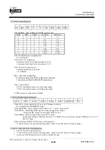
R5 = “xxxx0000”
IOC5 = "1111xx00"
R6 = PORT
IOC6 = "11111111"
R7 = PORT
IOC7 = "11111111"
R8 = PORT
IOC8 = "11111111"
R9 = PORT
IOC9 = "11111111"
RA = "000x0xxx
IOCA = "00000000"
RB = "11111111"
Page0 IOCB = "00000000"
Page1 IOCB = "00000000"
RC = "00000000"
Page0 IOCC = "0xxxxxxx"
Page1 IOCC = "00000000"
RD = "xxxxxxxx"
Page0 IOCD = "00000000"
Page1 IOCD = “00000000”
RE = "00000000"
Page0 IOCE = "00000010"
Page1 IOCE = "00000000"
RF = "00000000"
IOCF = "00000000"
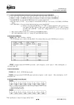
The controller can be awakened from SLEEP mode or IDLE mode (execution of "SLEP" instruction, named as
SLEEP MODE or IDLE mode) by (1)TCC time out (2) WDT time-out (if enabled) or, (3) external input at PORT9. The
three cases will cause the controller wake up and run from next instruction. After wake-up , user should control WATCH
DOG in case of reset in GREEN mode or NORMAL mode. The last two should be open RE register before into sleep
mode or IDLE mode . The first one case will set a flag in RF bit0 .But it will not go to address 0x08.
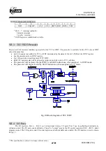
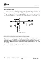
VII.6 Interrupt
The CALLER ID IC has internal interrupts which are falling edge triggered, as followed : TCC timer overflow
interrupt (internal) , two 8-bit counters overflow interrupt .
If these interrupt sources change signal from high to low , then RF register will generate '1' flag to corresponding
register if you enable IOCF register.
RF is the interrupt status register which records the interrupt request in flag bit. IOCF is the interrupt mask register.
Global interrupt is enabled by ENI instruction and is disabled by DISI instruction. When one of the interrupts (when enabled)
generated, will cause the next instruction to be fetched from address 008H. Once in the interrupt service routine the source
of the interrupt can be determined by polling the flag bits in the RF register. The interrupt flag bit must be cleared in
software before leaving the interrupt service routine and enabling interrupts to avoid recursive interrupts.
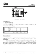
There are four external interrupt pins including INT0 , INT1 , INT2 , INT3 . And four internal interrupt available.
Internal signals include TCC,CNT1,CNT2,FSK and CALL WAITING data. The last two will generate a interrupt
when the data trasient from high to low.
External interrupt INT0 , INT1 , INT2 , INT3 signals are from PORT7 bit0 to bit3 . If IOCF is enable then these
signal will cause interrupt , or these signals will be treated as general input data .
After reset, the next instruction will be fetched from address 000H and the instruction inturrept is 001H and the
hardware inturrept is 008H.
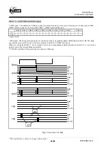
TCC will go to address 0x08 in GREEN mode or NORMAL mode after time out. And it will run next instruction
from “SLEP” instruction. These two cases will set a RF flag.
It is very important to save ACC,R3 and R5 when processing a interruption.
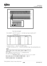
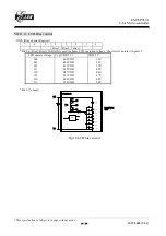
Address Instruction Note
0x08 DISI
;Disable
interrupt
0x09
MOV A_BUFFER,A
;Save ACC
0x0A
SWAP A_BUFFER
0x0B
SWAPA 0x03
;Save R3 status
0x0C
MOV R3_BUFFER,A
0x0D
MOV A,0x05
;Save ROM page register
0x0E
MOV R5_BUFFER,A
: :
: :
:
MOV A,R5_BUFFER ;Return R5
:
MOV 0X05,A
: SWAPA
R3_BUFFER
;Return
R3

