EM78P911A
8-bit Micro-controller
__________________________________________________________________________________________________________________________________________________________________
* This specification is subject to change without notice.
~ ~
23
12/19/2005 (V2.1)
VII.9 FSK FUNCTION
VII.9.1
Functional Block Diagram
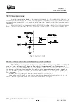
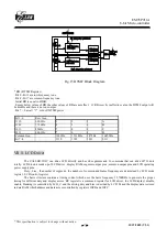
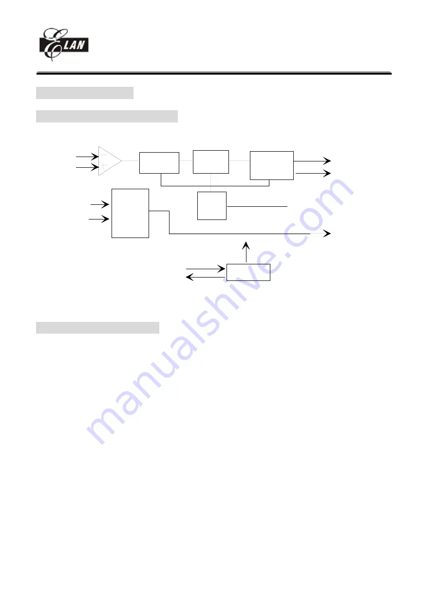
Fig.13 FSK Block Diagram
VII.9.2 Function Descriptions
The CALLER ID IC is a CMOS device designed to support the Caller Number Deliver feature which is offered by
the Regional Bell Operating Companies.The FSK block comprises two paths: the signal path and the ring indicator path. The
signal path consist of an input differential buffer,a band pass filter, an FSK demodulator and a data valid with carrier detect
circuit. The ring detector path includes a clock generator, a ring detect circuit .
In a typical application, the ring detector maintains the line continuously while all other functions of the chip are
inhibited. If a ring signal is sent, the /RINGTIME pin will has a low signal. User can use this signal to wake up whole chip or
read /RD signal from RA register.
A /FSKPWR input is provided to activate the block regardless of the presence of a power ring signal. If /FSKPWR
is sent low, the FSK block will power down whenever it detects a valid ring signal, it will power on when /FSKPWR is high.
The input buffer accepts a differential AC coupled input signal through the TIP and RING input and feeds this
signal to a band pass filter. Once the signal is filtered, the FSK demodulator decodes the information and sends it to a post
filter. The output data is then made available at DATA OUT pin. This data, as sent by the central office, includes the header
information (alternate "1" and "0") and 150 ms of marking which precedes the date , time and calling number. If no data is
present, the DATA OUT pin is held in a high state. This is accomplished by an carrier detect circuit which determines if the
in-band energy is high enough. If the incoming signal is valid and thus the demodulated data is transferred to DATA OUT
pin . If it is not, then the FSK demodulator is blocked.
Ring
Det
Circuit
Ring det1
Tip
Ring
Power
Up
FSK
demodul
Data Valid
Energy Det
Circuit
DATA OUT
/CD
CLOCK
OSC in
OSC out
/RD
/Ring Time
Band Pass
Filter
/FSKPWR


