background image


Back

of

Pot

Back

of

Pot

Back

of

Pot

Back

of

Pot

Back

of

Pot

Back

of

Pot

Back

of

Pot

Back

of

Pot

R1

Stage 1

50K Linear

R2

Stage 2

50K Linear

R3

Stage 3

50K Linear

R4

Stage 4

50K Linear

R5

Stage 5

50K Linear

R6

Stage 6

50K Linear

R7

Stage 7

50K Linear

R8

Stage 8

50K Linear

1 2 3 4 5 6 7 8

P207

Analogue Board J7


Figure 6-7:  P207 Programming Pot Connections 


Back

of

Pot

Back

of

Pot

Back

of

Pot

Back

of

Pot

Back

of

Pot

Back

of

Pot

Back

of

Pot

Back

of

Pot

R9

Stage 9

50K Linear

R10

Stage 10

50K Linear

R11

Stage 11

50K Linear

R12

Stage 12

50K Linear

R13

Stage 13

50K Linear

R14

Stage 14

50K Linear

R15

Stage 15

50K Linear

R16

Stage 16

50K Linear

1 2 3 4 5 6 7 8

P208

Analogue Board J8


Figure 6-8:  P208 Programming Pot Connections 


58

Summary of Contents for Klee Sequencer

Page 1: ...Building the electro music Klee Sequencer Issue 6 Copyright 2008 electro music com This document may be freely reproduced and distributed in its un altered form Cover photography by Tom Bugs a ...

Page 2: ...er 5 Building the Cables 40 Chapter 6 Installing the Panel PCB Wiring 53 Chapter 7 Building the Boards 69 Chapter 8 Final Assembly of the electro music Klee Sequencer 91 Chapter 9 electro music Klee Sequencer Bring Up Procedure 97 Chapter 10 Calibrating the electro music Klee Sequencer 109 Appendices Appendix A Analogue Board Bill of Material A1 Appendix B Digital Board Bill of Material B1 Appendi...

Page 3: ...ffect these outputs These outputs are useful for various reasons For example you may wish to control the cutoff of a filter with a slewed version Output A B yet control the VCO passing through the filter with a non slewed version of the same voltage The three optional outputs A A B and B are provided on J3 of the Analog Board on a six pin connector which includes the standard outputs Variable Rang...

Page 4: ...the position of the SPDT ON ON switch will determine if the maximum voltage is supplied internally by the Klee or by externally applied positive voltage Optional External Load Enable Switch The Optional External Load Enable Switch is an option that can be added to the front panel It merely consists of connecting the external load jack to a SPST On Off switch and connecting the output of the switch...

Page 5: ...s where indicated make an effort to match the resistors used to 0 1 To Use Connectors or Hardwire The Klee PCB board set has been set up to interface with the front panel through wire harnesses and sockets This makes assembly and troubleshooting much more of a breeze than hardwiring the connections It adds some time to construct the cables but saves in a lot of time and effort down the road The co...

Page 6: ... would apply to any project of yours Now you may be thinking That s all well and good but what flippin controls go on the damn thing in the first place That s cool That s a cool question The Klee Sequencer has a number of controls most sequencers have but it has a few that are perhaps not so common So we re going to introduce you to two things right now the first thing are the controls that allow ...

Page 7: ...Adjusts the voltage of Stage 12 Stage 13 Programming Pot Adjusts the voltage of Stage 13 Stage 14 Programming Pot Adjusts the voltage of Stage 14 Stage 15 Programming Pot Adjusts the voltage of Stage 15 Stage 16 Programming Pot Adjusts the voltage of Stage 16 Glide A Adjusts the glide of Voltage Output A Glide B Adjusts the glide of Voltage Output B Glide A B Adjusts the glide of Voltage Output A ...

Page 8: ...ts signal to Gate Bus 1 2 or 3 from Step 5 Gate Bus Switch 6 Directs signal to Gate Bus 1 2 or 3 from Step 6 Gate Bus Switch 7 Directs signal to Gate Bus 1 2 or 3 from Step 7 Gate Bus Switch 8 Directs signal to Gate Bus 1 2 or 3 from Step 8 Gate Bus Switch 9 Directs signal to Gate Bus 1 2 or 3 from Step 9 Gate Bus Switch 10 Directs signal to Gate Bus 1 2 or 3 from Step 10 Gate Bus Switch 11 Direct...

Page 9: ...stages Master Gate Outputs constant gate signal synchronous with clock Master Trigger Outputs constant trigger signal synchronous with clock Bus 1 Gate Outputs Gate Bus 1 gate signal Bus 1 Trigger Outputs Gate Bus 1 trigger signal Bus 2 Gate Outputs Gate Bus 2 gate signal Bus 2 Trigger Outputs Gate Bus 2 trigger signal Bus 3 Gate Outputs Gate Bus 3 gate signal Bus 3 Trigger Outputs Gate Bus 3 trig...

Page 10: ...and will generate a 1 if a rising clock signal is present Total Number of LEDs 22 General Recommended Guidelines We re not here to tell you how you should lay out your Klee panel In fact if you want to emboss strawberries and leprechauns on the panel power to you However there are some things we would consider helpful Try to keep the pattern LEDs clear of other LEDs For example if you put the gate...

Page 11: ... So do it now before you forget Remember the world of the back of the panel is a bizarre universe where everything is backwards left is right right is wrong clockwise is anticlockwise and up is often down Mark the stage numbers mark the label of the switch mark the positions of the switch Merge On Invert B etc You ll be glad you did says the Voice of Experience Orienting Testing and Mounting the P...

Page 12: ...losed it better now read open and vice versa If there is no change you either have the wrong type of switch or it s a bad switch and a bad idea to use it If there are more than two positions to the switch it s the wrong switch So what better tool is there than a table to tell you what position your switch must be in to do its thing Why nothing that s what Here s your table Closed shorted Position ...

Page 13: ...ontinuity tester and attach one lead to the center terminal on the back of the switch Hold the switch in the position you plan to mount it on the panel and flip the lever to the up position make sure it s not in the center position Connect the other lead of your DMM to the bottom terminal on the rear of the switch opposite of the Up direction you just flipped the switch You should now have a short...

Page 14: ...ion So once you ve determined you have a good set of the right switches for the gate bus group them all together and lay them aside Let s look at our one remaining oddball toggle switch the SPDT ON ON switch used for the Invert B Switch ON ON means that we have only two positions for this switch So if you have more than two positions all together now Wrong Switch Physically it looks the same as th...

Page 15: ...s the anode and which is the cathode Generally LEDs will have the longer lead as the anode and the shorter lead as the cathode The body of the LED will also give you a clue which is which it will have a flat side which will signify that s where the cathode is Flat Side Anode Cathode Figure 3 4 The LED Illustrated But let s be habitual and double check to be sure You ll need a DMM with a diode test...

Page 16: ... LEDs actually attain a very respectable brightness with that value The recommended high efficiency LEDs certainly perform very well also If you should decide that you think the value is too high and you decide you re going to lower it to get a really really bright display then that would be a bad decision in this case The health and longevity of your electro music Klee sequencer is dependent on t...

Page 17: ... two sections are separated by a non conducting ring on the plug When you plug one of these plugs into a jack the jack will provide the signal output on the tip lug of the jack and the ground reference on the ground lug of the jack So to check which lug is which plug a cable into your jack Now connect one lead of your DMM continuity tester to the tip of your cable and probe one lug of the jack If ...

Page 18: ... s still plugged into your jack to the ground of the cable that s plugged into your jack Repeat the process until you re sure which lug is the ground lug of your jack Ground Lug Tip Lug 0 00 Figure 3 8 Locating the Ground Lug Back to that third lug One option of the electro music Klee Sequencer called the Auto Switching External Internal Range Option number 3 on page 9 of the front panel interconn...

Page 19: ...n t find such a lug then your jack will not work with that option Ground Lug Tip Lug n c Switch Lug Figure 3 10 Cable Inserted N C Lug Open Now comes the time to mount the components Keep a few things in mind you probably want to mount the hardy components first the jacks switches and pots Then you ll probably want to attach and align your knobs and if you re really into this kind of stuff those c...

Page 20: ...Linear Panel Mount Pot Programming Pot 15 R15 50K Linear Panel Mount Pot Programming Pot 16 R16 50K Linear Panel Mount Pot Glide A R20 1M Linear Panel Mount Pot Glide B R21 1M Linear Panel Mount Pot Glide A B R19 1M Linear Panel Mount Pot Random Level R18 100K Linear Panel Mount Pot Random Reference R17 100K Linear Panel Mount Pot Optional Variable Range R22 100K Linear Panel Mount Pot Table 3 3 P...

Page 21: ...28 SPDT ON OFF ON Gate Bus Switch 13 SW29 SPDT ON OFF ON Gate Bus Switch 14 SW30 SPDT ON OFF ON Gate Bus Switch 15 SW31 SPDT ON OFF ON Gate Bus Switch 16 SW32 SPDT ON OFF ON Merge 1 Switch SW33 SPST ON OFF Merge 2 Switch SW34 SPST ON OFF Merge 3 Switch SW35 SPST ON OFF Bus 1 Load Switch SW36 SPST ON OFF Clock Enable Switch SW39 SPST ON OFF Rand Pat Switch SW41 SPST ON OFF 8X2 16X1 Switch SW40 SPST...

Page 22: ...r 3 5 mm Jack Table 3 7 LED Indicators Label Panel Des 300 Series Type Pattern LED 1 D1 High Efficiency Red LED Pattern LED 2 D2 High Efficiency Red LED Pattern LED 3 D3 High Efficiency Red LED Pattern LED 4 D4 High Efficiency Red LED Pattern LED 5 D5 High Efficiency Red LED Pattern LED 6 D6 High Efficiency Red LED Pattern LED 7 D7 High Efficiency Red LED Pattern LED 8 D8 High Efficiency Red LED P...

Page 23: ...with the same orientation comes in handy for strapping unless you use banana jacks in which case orientation does not apply Now before proceeding go back with your DMM and make sure your switches still work and are in the right position After that s all sorted Apply and align all knobs and accoutrements Mount the LEDs with a common orientation After you re done mounting the LEDs make sure they re ...

Page 24: ...ther This has the advantage of being insulated from inadvertent shorting to any other point but at the same time is a lot of work Bare bus wire on the other hand has the twin advantages of easily being soldered without stripping or tinning and allowing any point to be connected when it comes time to connect the common point to the PCB The disadvantage is it is not insulated Insulation can be purch...

Page 25: ...d Analog ground is used for all of the programming pots the optional external range components if used and all of the voltage output jacks Bus 1 connects to either the upper or lower terminal depending on your panel labeling of all of the gate bus switches AND the Bus 1 Load Switch Bus 3 connects to either the upper or lower terminal depending on your panel labeling of all of the gate bus switches...

Page 26: ... By now you ve already oriented them so they point to the right label on the front panel Now it doesn t matter if you connect the common ground to either the upper or lower terminal at the rear of the switch Since they re all in a line unless you have some cool circular panel going on it s easier to connect all the terminals together in a line Each switch will have only one of its terminals connec...

Page 27: ...Bus LED Figure 4 3 Strap Wiring Digital Ground to the Gate Bus LEDs o Gate Bus Jacks Banana jackers need not read this there is no ground connection for a banana jack All others connect the Gate Bus 1 Gate Bus 2 Gate Bus 3 and Master Gate Bus gate and trigger jacks together Make sure you know which terminal on your jack of choice is the ground terminal As usual this assumes your gate bus jacks are...

Page 28: ...nd to the Random Control Pots Connect the ground lug of the Random Reference and Random Signal Level pots to digital ground Remember you re in the bizarro world of the rear panel so the ground lug is to your right as you re looking at the panel o Clock Input Jack External Load Jack and Random Input Jack Banana jackers need not apply For all others connect the ground lug of the Clock Input Jack Ext...

Page 29: ...ust connect them to the nearest Digital Ground point on the panel Again these are the SPST ON OFF type so either terminal will do just make sure you have them aligned right on the panel as per the beginning of this screed Leave the other terminal of each switch open for wiring to the PCBs And lest you forget don t get those switches too hot The Final Step For Digital Ground Strapping make sure all...

Page 30: ...de Gate Bus 1 LED Cathode Gate Bus 2 LED Cathode Gate Bus 3 LED Cathode Pattern Switch 1 one lug connected Pattern Switch 2 one lug connected Pattern Switch 3 one lug connected Pattern Switch 4 one lug connected Pattern Switch 5 one lug connected Pattern Switch 6 one lug connected Pattern Switch 7 one lug connected Pattern Switch 8 one lug connected Pattern Switch 9 one lug connected Pattern Switc...

Page 31: ... Connected for non banana jack Bus 1 Gate Output Jack Ground Lug Connected for non banana jack Bus 1 Trigger Output Jack Ground Lug Connected for non banana jack Bus 2 Gate Output Jack Ground Lug Connected for non banana jack Bus 2 Trigger Output Jack Ground Lug Connected for non banana jack Bus 3 Gate Output Jack Ground Lug Connected for non banana jack Bus 3 Trigger Output Jack Ground Lug Connec...

Page 32: ...tage 16 50K Linear Figure 4 6 Strap Wiring Analog Ground to the Programming Pots o Voltage Output Jacks If you are not using banana jacks you ll need to connect the ground lugs of the Voltage Output A A B and B jacks together If you re also installing the Optional Voltage Output jacks you ll also need to connect the ground lugs of those jacks to Analog Ground Remember to be sure you know which lug...

Page 33: ...st Lug looking from back connected Programming Pot 7 Rightmost Lug looking from back connected Programming Pot 8 Rightmost Lug looking from back connected Programming Pot 9 Rightmost Lug looking from back connected Programming Pot 10 Rightmost Lug looking from back connected Programming Pot 11 Rightmost Lug looking from back connected Programming Pot 12 Rightmost Lug looking from back connected Pr...

Page 34: ...your legend on the panel is reversed you want to point down for Gate Bus 1 be sure to take this into account Also be sure your toggle switches work as described here If you re not sure re read the beginning sections of this procedure o Common Connections to the Gate Bus Switches Connect all of the top lugs of the switches together After that connect all of the bottom lugs of the switches together ...

Page 35: ...d Gate Bus 1 Load will be on So solder a wire from Bus 1 to one of the lugs of this switch Bus 1 Bus 3 SW36 Bus 1 Load SPST ON OFF Figure 4 9 Connecting the Bus 1 Load Switch To Bus 1 After you ve finished up wiring all of the Gate Bus Switches attach a lead of your DMM to the Bus 1 common connection and ensure that the switches all have a common connection with Bus 1 Make sure to check that the B...

Page 36: ...here is only one connection to a banana jack and this the one connection you need here Solder a wire between the tip lug or your single banana jack connection of the Random Signal Input Jack to the left most lug of the Random Level Pot as viewed from the back J14 Random Signal Input Ground Lug Back of Pot Tip Lug R18 Random Signal Level Figure 4 10 Wiring the Random Input to the Random Level Pot o...

Page 37: ... lug on the right So why connect the center tap to the lug on the left what does it accomplish Not a whole lot except that it serves as a form of protection should the pot suffer catastrophic failure and internally the center tap disconnects from the rest of the pot If this happens even without the wire put in nothing truly destructive would happen there wouldn t be any magic smoke or pretty flash...

Page 38: ...ble Switch It s an SPST ON OFF switch so for now you can connect it to either terminal of the switch If you didn t put in the optional switch drill a hole and put one in you ll find it s pretty handy Or not This option appears on page 6 of the front panel interconnect schematic J12 External Load Input Ground Lug Tip Lug SW345 Ext Load Enable SPST ON OFF Figure 4 13 Connecting External Load Input J...

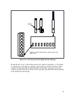
Page 39: ... External Range Input Jack to Variable Range Pot Opt 2 o Variable Range Option 3 Auto Switched Internal External Variable Range Those of you who do not use banana jacks this is your turn to chortle This option is not available if banana jacks are used It uses a normalled connection to actuate the function It requires either a 1 4 jack or a 3 5mm jack with a normally closed n c switch lug It is fro...

Page 40: ...anel real estate However before you non banana jackers giggle too much it should be mentioned this arrangement does provide a level of convenience greater than Option 3 For example if one is dynamically changing things during a Klee Sequence this allows one to switch between internal and external signals without having to physically remove the plug from the External Range Input Jack The strap conn...

Page 41: ... to find out it s still comparatively easy to change it out at this point This wraps up all of the notes about putting in the strap connections to the front panel Once these connections are made a good deal of the panel work is already done Now the only thing left to do with the front panel is to install the wires that will connect it to the PCBs themselves This is a good time to finish up that po...

Page 42: ...three elements The housing which is a shell that the cables are plugged into and which connects to the proper header on the PCBs There are different types of headers used in the electro music Klee Sequencer they differ by the number of wires they will accommodate The Klee uses 8 pin 6 pin 4 pin 3 pin and 2 pin headers The crimp terminals which are crimped or soldered or crimped and soldered to the...

Page 43: ...erted into the housing The terminals have a couple of tabs at the top that are intended to be crimped or folded over the insulation of the wire The end of the wire is stripped and tinned about from the end of the wire This stripped and tinned part is to extend down so the loop of the crimp terminal compresses down onto the bare wire when the wire and crimp terminal are inserted into the housing Cr...

Page 44: ...ires longer than what you think may be needed allows you to measure them out by physically stretching them to where your boards will be and ensuring they will indeed reach before you actually do solder them to the front panel You can break the job down into separate tasks For example you can go through task of stripping all of the wires needed and attaching the crimp terminals Then you can task yo...

Page 45: ...e Housing Once you ve got the terminal pins attached to your wires you can insert them into the housings When you insert the terminals into the housing make sure that little barb on the back of the terminal is oriented towards the side of the housing that has the small window in it the barb is designed to catch in that window like a hook in the mouth of a fish and make it harder for Gorilla Fist t...

Page 46: ... Remember that loop on the terminal must not be crushed or misshapen it is intended to compress down over the wire making a good connection and also provides a certain amount of tension that helps hold the terminal in the housing And again too much solder if you put solder on or solder in the wrong place can inhibit the actual installation of the terminal into the housing 44 ...

Page 47: ...rmation as to which pin must be connected to what on the panel The cables are named by the number the housing is assigned to a P followed by a designation The P means plug and the designation does have some useful information built into it as well The designation numbers come in two flavors they either start with a 1 such as P103 or they start with a 2 such as P204 Those designators that start wit...

Page 48: ...lock LED D321 Anode Pin7 Bus 1 Load Switch SW336 Pin8 Manual Step Switch SW337 P104 Pin1 Pattern Switch 8 SW308 Pin2 Pattern Switch 7 SW307 Pin3 Pattern Switch 6 SW306 Pin4 Pattern Switch 5 SW305 Pin5 Pattern Switch 4 SW304 Pin6 Pattern Switch 3 SW303 Pin7 Pattern Switch 2 SW302 Pin8 Pattern Switch 1 SW301 P105 Pin1 Pattern Switch 16 SW316 Pin2 Pattern Switch 15 SW315 Pin3 Pattern Switch 14 SW314 ...

Page 49: ...Switch 16 SW332 Center Lug Pin2 Gate Bus Switch 15 SW331 Center Lug Pin3 Gate Bus Switch 14 SW330 Center Lug Pin4 Gate Bus Switch 13 SW329 Center Lug Pin5 Gate Bus Switch 12 SW328 Center Lug Pin6 Gate Bus Switch 11 SW327 Center Lug Pin7 Gate Bus Switch 10 SW326 Center Lug Pin8 Gate Bus Switch 9 SW325 Center Lug P205 Pin1 Programming Pot 8 R308 Top Pin2 Programming Pot 7 R307 Top Pin3 Programming P...

Page 50: ... 16 R316 Center Pin2 Programming Pot 15 R315 Center Pin3 Programming Pot 14 R314 Center Pin4 Programming Pot 13 R313 Center Pin5 Programming Pot 12 R312 Center Pin6 Programming Pot 11 R311 Center Pin7 Programming Pot 10 R310 Center Pin8 Programming Pot 9 R309 Center P209 Pin1 Range Switch Pole Lug SW343 Pin2 Range Switch Throw 2 Lug SW343 Pin3 Range Switch Throw 3 Lug SW343 Pin4 Range Switch Throw...

Page 51: ...te Bus 3 LED D319 Anode Pin6 Gate Bus 3 Gate Jack J305 Tip Lug P212 Pin1 Glide B Pot R321 Center Tap Pin2 Glide B Pot R321 Top Pin3 Glide A Pot R320 Center Tap Pin4 Glide A Pot R320 Top Pin5 Glide A B Pot R319 Center Tap Pin6 Glide A B Pot R319 Top P213 Pin1 Output B Jack J315 Tip Lug Pin2 Optional Output B Jack J309 Tip Lug Pin3 Output A B Jack J316 Tip Lug Pin4 Optional Output A B Jack J310 Tip ...

Page 52: ...ch SW344 Outside Lug Pin2 Variable Range Pot R322 Center Tap Power Supply and Board Interconnect Cables While you re at it this is the perfect opportunity to build the remaining cables the cables used to connect the electro music Klee PCBs together and the cable required to connect to the power supply itself The power supply cable is similar to the front panel connect cables it has a housing on on...

Page 53: ...in one direction just as with all of the ICs This makes things easy to identify which pin is pin 1 on the PCBs It also means that from the vantage point of the housings that plug into them it requires you to remember that when the front side of a housing is pointing to you on one end of the wire the backside with the slots will be facing you when the cables are laid out straight in front of you Ta...

Page 54: ...he cables are put together you ll notice you have a nice pile of cables In that pile you will have 13 eight wire cables with a single housing 4 six wire cables with a single housing 1 four wire cable with a single housing 1 three wire cable with a single housing 2 two wire cables with a single housing or 3 of them if you are installing any of the variable range options 2 eight wire cables with hou...

Page 55: ...panel has already been strap wired Some connections may not jibe directly as illustrated with what you have already strap wired for example you may have strap wired to the top rear terminal of an SPST ON OFF switch as opposed to the bottom don t worry about those differences As described earlier in the panel mounting section which terminal is connected on those switches doesn t matter as long as t...

Page 56: ...size After you have cut each wire on the cable strip and tin the ends of the wires that will connect to the panel components Strip them about 1 4 from the end of the wire that s around 6 5 mm Again take care that you don t overheat the panel components as you solder Pay particular attention to soldering the switches and LEDs All connections to the LEDs will be to the anode of the LED Strap wiring ...

Page 57: ...DT ON OFF ON 1 2 3 4 5 6 7 8 P201 Analogue Board J1 Figure 6 1 P201 Gate Bus Switch Connections 1 2 3 4 5 6 7 8 P203 SW32 Stage 16 SPDT ON OFF ON SW31 Stage 15 SPDT ON OFF ON SW30 Stage 14 SPDT ON OFF ON SW29 Stage 13 SPDT ON OFF ON SW28 Stage 12 SPDT ON OFF ON SW27 Stage 11 SPDT ON OFF ON SW26 Stage 10 SPDT ON OFF ON SW25 Stage 9 SPDT ON OFF ON Analogue Board J3 Figure 6 2 P203 Gate Bus Switch Co...

Page 58: ...SPST ON OFF 1 2 3 4 5 6 7 8 P104 Digital Board J4 Figure 6 3 P104 Pattern Switch Connections SW9 Stage 9 SPST ON OFF SW10 Stage 10 SPST ON OFF SW11 Stage 11 SPST ON OFF SW12 Stage 12 SPST ON OFF SW13 Stage 13 SPST ON OFF SW14 Stage 14 SPST ON OFF SW15 Stage 15 SPST ON OFF SW16 Stage 16 SPST ON OFF 1 2 3 4 5 6 7 8 P105 Digital Board J5 Figure 6 4 P105 Pattern Switch Connections 56 ...

Page 59: ...0K Linear 1 2 3 4 5 6 7 8 P205 Analogue Board J5 Figure 6 5 P205 Programming Pot Connections Back of Pot Back of Pot Back of Pot Back of Pot Back of Pot Back of Pot Back of Pot Back of Pot R9 Stage 9 50K Linear R10 Stage 10 50K Linear R11 Stage 11 50K Linear R12 Stage 12 50K Linear R13 Stage 13 50K Linear R14 Stage 14 50K Linear R15 Stage 15 50K Linear R16 Stage 16 50K Linear 1 2 3 4 5 6 7 8 P206 ...

Page 60: ...0K Linear 1 2 3 4 5 6 7 8 P207 Analogue Board J7 Figure 6 7 P207 Programming Pot Connections Back of Pot Back of Pot Back of Pot Back of Pot Back of Pot Back of Pot Back of Pot Back of Pot R9 Stage 9 50K Linear R10 Stage 10 50K Linear R11 Stage 11 50K Linear R12 Stage 12 50K Linear R13 Stage 13 50K Linear R14 Stage 14 50K Linear R15 Stage 15 50K Linear R16 Stage 16 50K Linear 1 2 3 4 5 6 7 8 P208 ...

Page 61: ...tage 1 Red LED 1 2 3 4 5 6 7 8 P108 Digital Board J8 Figure 6 9 P108 Pattern LED Connections Anode Cathode D16 Stage 1 Red LED Anode Cathode D15 Stage 15 Red LED Anode Cathode D14 Stage 14 Red LED Anode Cathode D13 Stage 13 Red LED Anode Cathode D12 Stage 12 Red LED Anode Cathode D11 Stage 11 Red LED Anode Cathode D10 Stage 10 Red LED Anode Cathode D9 Stage 9 Red LED 1 2 3 4 5 6 7 8 P109 Digital B...

Page 62: ...PST ON OFF SW41 Random Pattern SPST ON OFF SW40 8X2 16X1 SPST ON OFF Anode Cathode D22 Random Reference Red LED Back of Pot R17 Reference Level 100K Linear Back of Pot R18 Random Level 100K Linear J13 Clock Input Ground Lug Tip Lug 1 2 3 4 5 6 7 8 P102 Standard Configuration External Load Enable Switch Option Installed Digital Board J2 Digital Board J2 Figure 6 11 P102 Connections Note if the Cloc...

Page 63: ...o on the back of your switch there are probably twelve pins around the outside of the switch and one pin in the middle instead of the eight pins around the outside of the switch shown here That is of course fine Just remember like everything else in Bizarro Rear Panel World the pin assignments will work backwards Make sure you verify which pins are selected shorted to the center pole pin with each...

Page 64: ... Stage 4 SPDT ON OFF ON SW19 Stage 3 SPDT ON OFF ON SW18 Stage 2 SPDT ON OFF ON SW17 Stage 1 SPDT ON OFF ON Gate Bus Switches Bus 1 Bus 3 Figure 6 13 P103 Connections A Note About P103 Digital Board J3 Connections You ll notice that pin 1 of P103 connects to the common connection of Bus 3 which should have been wired up when the panel strap connections were installed The same is true of pin 5 whic...

Page 65: ...de D18 Gate Bus 2 Red LED Anode Cathode D17 Gate Bus 1 Red LED Figure 6 14 P110 Connections J5 Gate Bus 3 Gate Ground Lug Tip Lug J6 Gate Bus 3 Trigger Ground Lug Tip Lug J8 Master Gate Bus Gate Ground Lug Tip Lug Digital Board J11 1 2 3 4 5 6 P111 J7 Master Gate Bus Trigger Ground Lug Tip Lug Anode Cathode D20 Master Gate Bus Red LED Anode Cathode D19 Gate Bus 3 Red LED Figure 6 15 P111 Connectio...

Page 66: ...near 1 2 3 4 5 6 P212 Figure 6 16 P212 Connections J11 Optional A Ground Lug Tip Lug J10 Optional A B Ground Lug Tip Lug J9 Optional B Ground Lug Tip Lug J15 Output B Ground Lug Tip Lug Analogue Board J13 1 2 3 4 5 6 P213 J16 Output A B Ground Lug Tip Lug J17 Output A Ground Lug Tip Lug Figure 6 17 P213 Connections 64 ...

Page 67: ... Invert B Mode On Digital Board J12 1 2 3 P112 SW42 Invert B SPDT ON ON Switch Lever Up Invert B Mode Off Figure 6 18 P112 Connections Back of Pot R17 Reference Level 100K Linear Digital Board J13 1 2 P113 Digital Ground Common Connection Figure 6 19 P113 Connections 65 ...

Page 68: ...le perhaps on the Digital Ground line connecting the pattern switches or pattern LEDs together Analogue Board J15 1 2 P215 Analog Ground Common Connection Figure 6 20 P215 Connections The Analog Ground of P215 which is the only signal carried by P215 should connect to a single point on the strap wired analog ground system of the front panel Again a good place would be centrally located perhaps on ...

Page 69: ...7 Variable Range 100K Linear Analogue Board J16 1 2 P216 Auto Switching Internal External Variable Range Option Option 3 Ground Lug Tip Lug n c Switch Lug J18 External Range In Back of Pot R17 Variable Range 100K Linear Analogue Board J16 1 2 P216 Manually Switched Internal External Variable Range Option Option 4 SW44 Internal External Variable Range Select SPDT ON ON Switch Up Selects External Fi...

Page 70: ...e in the up position simply wire the connection from Pin 1 to the opposite terminal refer to Figure 4 16 Once the cables are installed take the time to neaten them up twist them up into single cables or tie wrap them together Are the plugs labeled If not go through and label them Snip any LED leads that may be too long Maybe go through and check your switches Congratulations The most work intensiv...

Page 71: ... the gate and trigger signals the Klee will produce You the builder and owner of the Klee may have a preference as to these levels The Klee will produce either 5V range gate and trigger signals or 10V range gate and trigger signals The values used for these resistors will determine what gate trigger voltages you end up with There are no jumper wires that need be installed on the Digital Board Anal...

Page 72: ...Figure 7 1 The electro music Klee Sequencer Digital Board 70 ...

Page 73: ...g flatly on the board Make sure when you solder in the connectors they do indeed sit flatly on the board not jutting at some obscene angle like a badly rooted incisor A handy if somewhat potentially painful method of doing this is to put a dab of solder on the tip of your iron place the jumper into position and while holding it anchor one pin down with your dab of solder The painful part is if you...

Page 74: ...r art so what s a burned finger in the grand scheme of things Again your IC sockets will probably be keyed to go in a certain direction telling you which way to install the IC when the time comes Be sure to install them pointing in the right direction As a point of interest you ll notice the intrepid board designer designed the Klee PCBs with all of the ICs and connectors in the same direction whe...

Page 75: ...time to install the resistors Before we even go there we should first consider what level the gate bus gate and trigger signals will be And then we ll install those resistors first and have all of that sordid business behind us There are sixteen resistors that determine this now much ballyhooed level Eight of them should be of a single value and the other eight should be of a different single valu...

Page 76: ...t this is for 15V operation only For 12V operation the values will have to be different yet These values provide a 1K output impedance Note that the terms 5V range and 10V range are used here The actual voltages these resistor combinations will produce are 4 5V and 9V respectively During prototype testing these values were found to be compatible with all the equipment the Klee was interfaced to If...

Page 77: ...installing the gate bus resistors install the rest of the resistors Perhaps the best method is to gather all of the 100K resistors and install those then the 22K resistors and so forth Remember if you ve got 100K 0 1 resistors for your Analogue Board don t install them on this board This board ain t so picky and it would be an entire waste to do so Gate Bus Resistors Group 1 Selected Value Quantit...

Page 78: ...u install them in the right direction The silkscreen will show where the cathode goes 1N4148 Diodes Quantity Designators Type Done 7 D1 D7 Diode Si Capacitors There are a number of capacitors of various values Most of them are non polarized There is only one polarized capacitor on the Digital Board C17 When you install it be sure to do it in the right direction The positive lead of the cap will go...

Page 79: ...ilk screening serves as the guide to correct orientation of the transistors 2N3904 NPN Transistors Quantity Designators Type Done 6 Q1 Q6 NPN This covers all of the components that are soldered into the Digital PCB At this point go ahead and clean off the flux using your preferred method chemical Installing the ICs After the board is cleaned it s time to install the ICs into the sockets Remember f...

Page 80: ...t OR Gate 3 U4 U12 U13 CD4093 Quad 2 Input NAND Schmitt Trigger 1 U5 CD4013 Dual D Flip Flop 2 U6 U7 CD4034 8 Bit Shift Register with Parallel Load 1 U9 CD4053 Quad 1 of 2 Switch 2 U14 U15 LM324 Quad Op Amp CD4053 CD4034 CD4034 CD40106 CD40106 CD40106 LM324 LM324 LM358 LM358 CD4071 CD4093 CD4093 CD4093 CD4013 Figure 7 4 Digital Board IC Placement Guide 78 ...

Page 81: ...Figure 7 5 The electro music Klee Sequencer Analogue Board 79 ...

Page 82: ...e reason has only one ground connection In other words if you have a power supply with only one ground lead install W1 This ties the analog and digital grounds together at this one point The only other jumper W2 is only installed if any of the variable range options are not installed If you intend position 8 of the range to access only a fixed range and there is no other control to vary that range...

Page 83: ...ations If any of the variable range options are installed then you should refrain from installing R41 The front panel Variable Range Control will take over the function performed by that trim pot J16 must be installed unless of course you are hardwiring the Klee together J16 provides the signal s to the front panel Variable Range control s If any of the external range options are to be installed D...

Page 84: ...ust Be Installed Select Value For R33 Figure 7 8 Range Switch Position 8 Variable Range Considerations Resistors The default value for R33 is 1K it is used if the standard 8V fixed range is selected as the function of position 8 of the rotary Range Switch If you decide to install any of the internal variable range options R33 is going to determine the maximum voltage that can be dialed in with the...

Page 85: ...values ranges 1 through 3 are adjustable from 0V through 0 625V Range 4 is adjustable through 1 28V with the standard values Ranges 5 through seven are adjustable through 5V with the standard values and Range 8 is adjustable through 8 1V If one changes any of the divider resistor values for these ranges R26 through R33 it is possible to exceed these ranges The equation is as follows 10V Rdivider 1...

Page 86: ... R33 100K X 100K Maximum Range Figure 7 10 Equation for Maximum Variable Range Voltage Table 7 2 lists a general range of values for R33 and the resulting maximum variable range voltage each provides R33 Maximum Range 910K 0 99V 400K 2V 300K 2 5V 200K 3 33V 150K 4V 100K 5V 56K 6 4V 39K 7 2V Table 7 2 Example R33 Values and Resulting Maximum Variable Range Voltage If one settles for a lower variabl...

Page 87: ...d 0 1 resistors can be quite expensive If you have them or can afford acquire them this will make things much more cut and dried If not it is possible to match a set of resistors to within 0 1 1 metal film resistors can be purchased quite inexpensively these days Because of that it is possible to buy a large quantity of them for a relatively low price If you purchase a large quantity you will more...

Page 88: ... astutely determine that no J14 is listed rest assured it does not exist That reference designator was removed during development of the PCB 8 Pin Headers Quantity Designators Done 9 J1 J9 6 Pin Headers Quantity Designators Done 2 J12 J13 4 Pin Headers Quantity Designators Done 1 J10 2 Pin Headers Quantity Designators Done 2 3 J11 J15 J16 for Optional Variable Range IC Sockets Next install the soc...

Page 89: ...ing of this section again Come on it s not that bad 100R Resistors Quantity Designators Tol Done 9 R49 R57 5 1 4W 1K Resistors Quantity Designators Tol Done 1 R33 See notes at beginning of this section 5 1 4W 10K Resistors Quantity Designators Tol Done 3 R30 R32 1 1 4W 100K Resistors Quantity Designators Tol Done 25 R1 R25 0 1 150K Resistors Quantity Designators Tol Done 3 R26 R28 See notes at beg...

Page 90: ...ith a 1N4148 or 1N914 Install them in the right direction cathode is marked on the silkscreen 1N4148 Diodes Quantity Designators Type Done 28 D1 D28 Diode Si 1N4001 Diodes Quantity Designators Type Done 1 D29 Diode Si BAT85 Diodes Quantity Designators Type Done 1 D30 Schottky Diode Si Capacitors There are five capacitors on the Analogue Board that are polarized All of these are the electrolytic ca...

Page 91: ...4 R41 do not install R41 if variable range option is installed 25 Turn Top Adjust 100K Multi Turn Trim Pots Quantity Designators Type Done 2 R42 R43 25 Turn Top Adjust Installing the ICS All of the ICs are socketed save for one U5 the 78L10 Voltage Regulator Locate its position on the silk screening and install it in the orientation depicted on the silkscreen of the board 78L10 Quantity Designator...

Page 92: ...Designators Type Done 4 U1 U4 CD4066 Quad Analog Bi Lateral Switch 1 U6 TL072 Dual Op Amp 1 U7 CD4051 1 of 8 Analog Mux 3 U8 U10 TL074 Quad Op Amp TL074 TL074 TL074 TL072 CD4051 CD4066 CD4066 CD4066 CD4066 Figure 7 11 Analogue Board IC Placement Guide 90 ...

Page 93: ... it sure may head some problems off at the pass Checking the connections before the board is connected to anything else will immediately tell you if a problem exists on the board now before everything else gets involved causing a problem to be much more difficult to trace Visual Inspection Grab a magnifying glass and give the back of your board at least a cursory check keep an eye open for any sol...

Page 94: ...s interminable suspenseful procedure Check the IC Positive Power Pins The Digital Board is an easy easy board to check to see if the ICs are connected up to the rails mainly because there is only V and ground on the Digital Board A beeping continuity checker is great for this job Leave the positive lead of the DMM connected to pin 1 of J1 and begin checking the supply pins of each and every one of...

Page 95: ...s the Analogue Board It s the same drill Visually inspect the solder joints Visually inspect the socketed ICs Visually inspect the orientation of polarized parts transistors all those polarized caps all of those diodes Check for Power Supply Shorts The Analogue Board not only has two power rails to check but also two ground systems as well On top of that it s probably a good idea to make sure that...

Page 96: ...ve lead to pin 2 of J11 If it reads zero ohms or something tantamount to zero ohms your Digital Ground signal should make the trip between boards For those who have installed W1 on the Analog Board connect the positive lead to pin 2 of J10 and the negative lead to Pin 2 of J11 If you get zero ohms or something ludicrously close to it your W1 jumper is well soldered and good to go analog ground and...

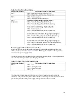
Page 97: ...78L10 Pin 2 U7 CD4051 Pin 8 Table 8 5 Analogue Board IC Ground Pins Check the Power Supply Before connecting everything up double check the power supply connection The P210 cable should be connected to the power supply terminals Power on the supply with it connected to nothing Ensure that there is 15V on pin 1 ground on pins 2 and 3 if there are two ground connections and 15V is on pin 4 of P210 O...

Page 98: ...which cable is which Chapter 5 should give you enough direction to figure out which is which If you re hardwiring you can go back to Chapter 5 and start soldering Connect all the P2XX cables to their respective connector on the Analogue Board Connect all the P1XX cables to the Digital Board In case you ve forgotten J205 connects to J5 Analogue Board J103 connects to J3 Digital Board and so on Afte...

Page 99: ... all possible Begin the Bring Up procedure by having nothing other than power connected to the Klee Powering Up the electro music Klee Sequencer This is the initial moment of truth apply power to the Klee by powering on the power supply Keep an eye peeled for wisps of smoke flashes of light If there are neither coming from the boards or power supply this is a good thing Note You may or may not get...

Page 100: ...ing controls 8X2 16X1 Switch 16X1 position Random Pattern Switch Pattern Position Invert B Switch OFF Clock Enable ON Pattern Switch 1 ON Pattern Switches 2 through 16 OFF Gate Bus 1 Load Switch OFF Press the Manual Load Switch The Stage 1 Pattern LED should illuminate all other Pattern LEDs should remain off Connect an LFO signal to the Clock Input Jack The Clock LED should begin flashing If it s...

Page 101: ...tern Switch to OFF or 0 Set the Stage 9 Pattern Switch to ON or 1 Press the Manual Load Switch Pattern LED 9 should illuminate and all other pattern LEDs should be off Set Clock Enable to ON The pattern LEDs for stages 9 through 16 should repeatedly cycle and the pattern LEDs 1 through 8 should remain off Testing the Invert B Function Continuing from the previous procedure Set Clock Enable to OFF ...

Page 102: ...Ds should cycle from Stage 1 through Stage 16 advancing one step each time the Manual Step Switch is pressed Testing the Gate Bus Switches Merge Switches and LEDs Continuing from the previous procedure Set all of the Gate Bus Switches to Gate Bus 2 middle position Set all merge switches to the OFF position Press the Manual Load switch Pattern LED 1 should illuminate all others should be off Set Cl...

Page 103: ...Gate Bus 3 Set Clock Enable to ON The Master Gate Bus LED should flash with each clock pulse The Gate Bus 3 LED should flash with each clock pulse The Gate Bus 1 LED and the Gate Bus 2 LED should both remain off Set the Merge 3 Switch to ON The Master Gate Bus LED should flash with each clock pulse and the Gate Bus 3 LED should stay constantly illuminated with no flashing The Gate Bus 1 and Gate B...

Page 104: ...erve the Random Reference LED it should remain illuminated Slowly turn the Random Reference Level clockwise the Random Reference LED should turn off Set the Random Pattern Switch to RANDOM Observe the pattern LEDs The illuminated Pattern LED will not recycle once it has stepped past Stage 16 After that the LEDs will remain off Turn the Random Level Control fully Clockwise Set the Random Signal Lev...

Page 105: ...V range or 10V range should appear with every flash of the Master Gate Bus LED If an oscilloscope is not available connect a trigger able device such as a drum voice or an envelope generator to the Master Gate Bus Trigger Output The device should trigger with each flash of the Master Gate Bus LED If an oscilloscope is available connect the oscilloscope to the Master Gate Bus Gate Output A pulse si...

Page 106: ...Bus 1 LED remains on for as long as the clock LFO is high If an oscilloscope is not available connect a gate able device to the Gate Bus 1 Gate Output This device could be an envelope generator or a VCA passing a signal Ensure the device stays gated as long as the Gate Bus 1 LED is on Gate Bus 2 Continuing from the previous procedure Set a number of Gate Bus Switches to Gate Bus 2 so that the Gate...

Page 107: ...tput A 1 ms wide signal at the selected gate bus voltage 5V range or 10V range should appear with every flash of the Gate Bus 3 LED If an oscilloscope is not available connect a trigger able device such as a drum voice or an envelope generator to the Gate Bus 3 Trigger Output The device should trigger with each flash of the Gate Bus 3 LED If an oscilloscope is available connect the oscilloscope to...

Page 108: ...stages 1 through 8 and will shift to a solid low pitch as the LED steps through stages 9 through 16 Turn the Glide A B control from full anti clockwise to clockwise Listen to the transitions from low to high and high to low the change between pitches should now not be abrupt but glide from one to the other The more clockwise the Glide A B control is the longer the glide time between the two pitche...

Page 109: ...tional A Output The change in pitch should be abrupt and unaffected by the setting of the Glide A Control Set Glide A to full anti clockwise B Output Glide B Control Continuing from the previous procedure Connect the VCO control to the B Output As the LEDs step the single bit through stages 1 through 8 the pitch of the VCO should stay a constant low As the LEDs step through stages 9 through 16 the...

Page 110: ...not installed the Optional External Variable Range Option you can sit out this procedure If you haven t done so set the programming pots so that each produces a pitch variation or rather just don t have them sitting full anti clockwise Connect the VCO V Oct control input to the A B Output Set the Variable Range Control to full anti clockwise Set the Range Switch to position 8 The pitch of the VCO ...

Page 111: ...idating number of trim pots This procedure will address the standard voltage arrangement reflected in the schematic If you decide you would like different voltages for the various positions of the Range Switch check out the Analogue Board section of Chapter 7 Required Tools A digital volt meter DVM is the only piece of test equipment required for the calibration Of course you ll need a trim pot ad...

Page 112: ...alog ground A good place to connect it would be somewhere on the analog ground system of the panel say the ground lug of one of the programming pots Adjust R42 Adjust for 0V at Pin1 of U8 Figure 10 1 Register A Offset Zero Calibration Register A Voltage Offset Zero Trim Touch the tip of the positive DVM lead to pin 1 of U8 While observing the DVM adjust R42 for 0V on the DVM Get as close to absolu...

Page 113: ...librations and is performed only after the offset zero calibrations have been completed All measurements are taken from pin 1 of U8 It uses the same setup as the offset zero with a couple of extra settings The goal of the calibration is to adjust the output voltage of one stage for each position of the rotary Range Switch The calibration begins with Range Switch position 1 full anti clockwise posi...

Page 114: ...ress the Manual Load Switch so that only the Stage 1 LED is illuminated Rotate the Stage 1 Programming Pot to full CW Ensure Programming Pots 2 through 16 are all set full anti clockwise Refer to Table 10 1 and adjust trim pots so that the voltage at pin 1 of U8 to the exact voltage listed for each position of the Range Switch Range Switch Position Trim Pot U8 Pin 1 Voltage 1 R34 0 333V 2 R35 0 41...

Page 115: ...c 330 nF 0 33 uF 1 C9 Ceramic 10 uF 2 C19 C20 Electrolytic 25V 4 7 uF 3 C10 C12 Electrolytic 25V Trim Pots Value Quantity Designators Type 10K 8 R34 R41 25 Turn Top Adjust 100K 2 R42 R43 25 Turn Top Adjust Diodes Value Quantity Designators Description 1N4148 28 D1 D28 Diode Si 1N4001 1 D29 Diode Si BAT85 1 D30 Schottky Si Integrated Circuits Device Quantity Designators Description 78L10 1 U5 10V L...

Page 116: ...n DIP 1 X6 0 3 Header Connectors Number of Pins Quantity Designators Description 8 9 J1 J9 Sip Header 0 1 Center 6 2 J12 J13 Sip Header 0 1 Center 4 1 J10 Sip Header 0 1 Center Sip Header 0 1 Center 2 2 3 J11 J15 J16 J16 for Optional Variable Range PCB electro music Klee Sequencer Analogue PCB A 2 ...

Page 117: ...28 5 1 4W 270K 1 R91 5 1 4W 3K 8 R63 R70 5 1 4W 4K7 6 R31 R48 5 1 4W R85 R88 6K8 16 R32 R47 5 1 4W Capacitors Value Quantity Designators Type 1 nF 001 uF 6 C6 C10 C18 Metal Poly 10 nF 4 C19 C22 Metal Poly 100 nF 0 1 uF 15 C1 C5 C13 C16 C23 C28 Ceramic 47 nF 047 uF 2 C11 C12 Metal Poly 47 uF 1 C17 Electrolytic 25V Diodes Value Quantity Designators Description 1N4148 7 D1 D7 Diode Si Transistors Val...

Page 118: ...Quad 2 Input NAND Schmitt Trigger LM324 2 U14 U15 Quad Op Amp LM358 2 U1 U8 Dual Op Amp IC Sockets Type Quantity Designators Width 24 Pin DIP 2 X6 X7 0 6 16 Pin DIP 1 X9 0 3 14 Pin DIP 10 X2 X5 X10 X15 0 3 8 Pin DIP 2 X1 X8 0 3 Header Connectors Number of Pins Quantity Designators Description 8 8 J2 J9 Sip Header 0 1 Center 6 2 J10 J11 Sip Header 0 1 Center 3 1 J12 Sip Header 0 1 Center 2 2 J1 J13...

Page 119: ... ON OFF Rotary 1 SW43 SP8T Optional Parts Potentiometers Type Quantity Designators Description Rotary Slide 16 R1 R16 50K Linear Panel Mount Rotary 3 R17 R18 R22 100K Linear Panel Mount Rotary 3 R19 R21 1M Linear Panel Mount Optional Parts LEDs Type Quantity Designators Description Red 20 D1 D20 High Efficiency Jacks Type Quantity Designators Description J1 J16 J17 Tip Connection 17 1 4 3 5mm Bana...

Page 120: ...212 P213 Connector Housing 6 Pos 4 Pin 1 P210 Connector Housing 4 Pos 3 Pin 1 P112 Connector Housing 3 Pos 2 Pin 5 P101 P113 P211 P215 P216 Connector Housing 2 Pos Optional Parts Crimp Terminals Type Quantity Designators Description Female Crimp Terminal 177 N A Connector Term Female 22 30 AWG Additional Items Front Panel Stranded Wire 22 24 AWG C 2 ...

Reviews: