


Jupiter
EVM
Getting
Started
Rev
C01
:
05/17/2007
Copyright
Elevate Semiconductor 2012
Page 18 of 22
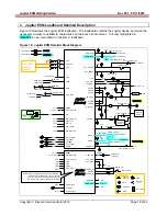
3
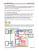
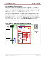
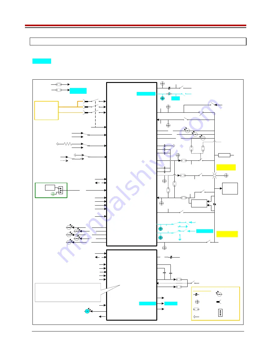
Jupiter EVM Loadboard Detailed Description
Figure 10 illustrates the Jupiter EVM loadboard. The loadboard contains the Jupiter device as well as the
necessary circuitry to validate & characterize on the bench environment. Circuitry highlighted in
turquoise is new or modified on the Rev C loadboard.
Figure 10: Jupiter EVM Detailed Block Diagram
TC5
VFORCE
TESTNODE
MB
Jupiter
(Master)
CLK/SDIO/STB
RESET
3
E2
TC17
Latch
TC_17
EN
FORCE_A
SENSE
Resistor
Network
CON_ES_TN
CON_VFORCE_EF
VFORCE
CON_EF_TN
MONITOR
EXT_SENSE
EXT_FORCE
TestNode(p)
VREF
VREF_SEL
VREF (DPS)
TestNode(p)
TC_10/2/3
TC_4
DUT_GND
TestNode(p)
GANG[1:0]
CON_GANG[1:0]_TN
VDD
CH3_FORCE
CH1_FORCE
A/D
CON _MON _TN
EXT_MON_OE
TC23
VFORCE
DUT_GND_SEL
VCC
External
Power
Supply
VCCOUT
VEE
V+
V-
EXT_ADDR_CK
TC18
EXT_U/D*
TC19
A/D
E4
FORCE_B
CON_SENSE_TN
CON_FB_TN
CAP_BP
CAP_AP
E3
E8
TESTNODE(p)
A/D
DPS_EN*
TC6
CAP_DIS*
TC8
C_BIT
Tj
CON_TJ_TN
A/D
Jupiter
(Slave)
CLK/SDIO/STB
RESET
3
TC_10/2/24
TC_25
VCC / VCCOUT
VEE
VDD
VCC
VEE
VDD
DUT_GND
GND
VREF
VREF
GANG[3:0]
(4)
E11
FORCE_A
SENSE
CON_SLAVE_TN
E5
FORCE_B
CAP_A/BP
CAP_A/BN
x2
x2
TEST_NODE
All Slave (Gang) supplies and input/output signals are
isolated from the Master via a switch, channel
protector, and/or use a dedicated control signal .
Use SLAVE_EN (CBit4) to enable the switches.
Digital Inputs
GND
Digital Outputs
N/C
MONITOR
A/D
Tj
A/D
A/D
A/D
A/D
REXT
REXT_SEL
TestNode(p)
10K
EXT_LD
TC20
EXT_TJ_EN
TC21
ALARM*
TC9
I_ALARM*
TC12
KEL_ALARM*
TC14
OT_ALARM*
TC11
V_ALARM*
TC13
CAP_SR
CAP_AN
CAN_BN
E7
Capacitor
Network
E10
E9
CON_FA_TN
Div2
A/D
GANG2
VFORCE2
GANG0
A/D
Channel
Protector
SMA
2-Pin Jmpr
GND
3-Pin Jmpr
Banana
Jack
LED
Symbol Legend
ALARM*
MON_REF
A/D
MON_REF
TestNode(p)
A/D
CON _MON_REF_TN
GANG3_SEL
GANG3
VFORCE
VFORCE2
CH5_FORCE
A/D
A/D
CON_GANG3_VF
CON_GANG2_VF2
GANG[3:0]
(Master)
GANG2_SEL


