Embedded Planet, Inc.
epConnected Asset | Product User Manual
Document Version: 1.0.0 | 26 Jan 22
Embedded Planet, Inc. | 31225 Bainbridge Rd Suite N, Solon, OH 44139 | 216-245-4180 | www.embeddedplanet.com |
Page 24 of 37
14.2.
Mini-Tectonic Edge
™
Pinout
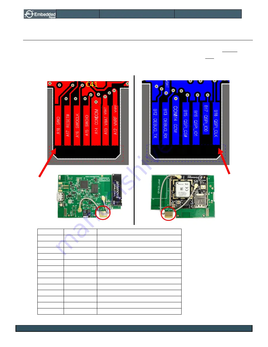
In the diagrams below, the red (left) represents the side of the epConnected Asset board
without
the
Chronos module, while the blue (right) represents the side of epConnected Asset board
with
the Chronos
module. Both diagrams are shown looking at the side of interest shown in the image below it. Note that the
board reverses its x-axis with the change in view sides, as if the physical board itself was being flipped over.
TABLE 8
–
MINI-TECTONIC EDGE
™
PINOUT
Pin
Direction
Description
SWO
Output
Single wire debug output
RESET#
Input
nRF52840 reset, active low
SWDCLK
Input
Single wire debug clock
SWDIO
I/O
Single wire debug data
COM
n/a
Board common
VBAT
Power Input
3.4V to 4.2V input to power the board
VnRF
Power Output 3.0V reference output from nRF52840
DEBUG_TX Output
Debug UART output (see below)
DEBUG_RX Input
Debug UART input (see below)
QSPI_CS#
Input
QSPI flash chip select, active low
QSPI_IO1
Output
QSPI flash single SPI data out
QSPI_IO0
Input
QSPI flash single SPI data in
QSPI_CLK
Input
QSPI flash clock
Pin A18
Pin A18
Summary of Contents for epConnected Asset
Page 10: ...5 Block Diagram ...


