
SMARC T335x Carrier Board Hardware Design Guide, Document Revision 1.2
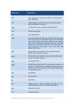
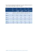
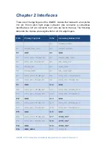
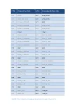
1.2 Signal Table Terminology
Table below describes the terminology used in this section for the Signal
Description tables.
The “
#
” symbol at the end of the signal name indicates that the active or
asserted state occurs when the signal is at a low voltage level. When “
#
” is not
present, the signal is asserted when at a high voltage level.
Direction
Type / Tolerance
Notes
Input
Input to the Module
Output
Output from the Module
Output
OD
Open drain output from the Module
Bi
‐
Dir
Bi-directional signal (can be input or output)
Bi
‐
Dir
OD
Bi-directional signal; output from the Module is
open drain
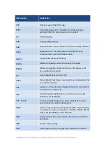
VDD_IN
Signal may be exposed to Module input voltage
range (3.35 to 5.25V)
CMOS 1.8V
CMOS logic input and / or output, 1.8V I/O supply
level or tolerance
CMOS 3.3V
CMOS logic input and / or output, 3.3V I/O supply
level or tolerance
CMOS
VDD_IO
CMOS logic I/O level – set to 3.3V for SMATC
T335X Modules
CMOS
VDD_JTAG_IO
VDD_JTAG_IO is 3.3V in SMARC T335X. The
JTAG emulator adjusts to the VDD_JTAG_IO level
provided by the Module, on the JTAG connector
GBE MDI
Differential analog signaling for Gigabit Media
Dependent Interface
LVDS AFB
LVDS signaling for AFB – may be PCIe, SATA,
USB SS, GBE MDI, MLB or other low voltage high
speed differential physical interface