Functional Description
ATCA-F120 Installation and Use (6806800D06F
)
80
4.2
Block Diagram
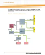
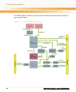
The following figure provides an overview of the main function blocks of the ATCA-F120 and
how they are interconnected.
4.3
Central Processing Unit
The blade’s Central Processing Unit (CPU) is a MPC8548E PowerQUICC III processor. It supports
CPU speeds of 1000 MHz, 1200 MHz and 1333 MHz. On the ATCA-F120, the default CPU speed
is 1333 MHz.
Figure 4-1
Block Diagram
Fabric Interface
2 x 10G
4 x 1G
1G
F
ace
P
late
1G to
partner’s BIX
1G to partner’s PrAMC
4x 1G
AMC
Bay B4
PowerQUICC
CPU
MPC
8548E
RAM
Flash
1G
IPMC /
ShMC
10/100 to
partner’s BBP
1G Mgmt
PCI
AMC
Bay B1
x4 PCIe
2x SAS/SATA
Dual
Block Transfer
15 x 1/10G
15 x 1G
1G to
partner’s PrAMC
Base Interface
IPMBs
RT
M
4 x 10G
Base
Interface
Switch
BCM56502
24 x 1G
2 x 10G
1G
10/100 to SAM
5 x 1G
Dual
MAC
1G
x4
PCIe
RS232
1G
Base
Interface
Switch
Extender
BCM5385
1G
Telecom
Clock
Support
2x Extension Shelf
3x Telecom Clocks
RS232 to
partner’s BBP
10/100 to SAM
BC1
BC1
UC0
UC1
Fabric
Interface
Switch #1
BCM56800
20 x 10G
Fabric
Interface
Switch #2
BCM56502
2 x 10G
24 x 1G
1 x HiGig
1G
1G
Ba
ckplane
UC3/2
UC2/3
UC4
CLK
Glue Logic
FPGA
Summary of Contents for ATCA-F120
Page 6: ...ATCA F120 Installation and Use 6806800D06F Contents 6 Contents Contents ...
Page 8: ...ATCA F120 Installation and Use 6806800D06F 8 List of Tables ...
Page 10: ...ATCA F120 Installation and Use 6806800D06F 10 List of Figures ...
Page 18: ...ATCA F120 Installation and Use 6806800D06F About this Manual 18 About this Manual ...
Page 24: ...ATCA F120 Installation and Use 6806800D06F Safety Notes 24 ...
Page 120: ...U Boot Firmware ATCA F120 Installation and Use 6806800D06F 120 ...
Page 124: ...Index ATCA F120 Installation and Use 6806800D06F 124 ...
Page 125: ......


