background image

2-4

LTVN_ISP

Safety Check after Servicing

Examine the area surrounding the repaired location for damage or deterioration. Observe that screws, parts and 
wires have been returned to original positions. Afterwards, perform the following tests and confirm the specified 
values in order to verify compliance with safety standards.

1. Clearance Distance

When replacing primary circuit components, confirm 
specified clearance distance (d) and (d') between 
soldered terminals, and between terminals and 
surrounding metallic parts. (See Fig. 1)

Table 1: Ratings for selected area

Note:

  This table is unofficial and for reference only. Be 

sure to confirm the precise values.

2. Leakage Current Test

Confirm the specified (or lower) leakage current 
between B (earth ground, power cord plug prongs) and 
externally exposed accessible parts (RF terminals, 
antenna terminals, video and audio input and output 
terminals, microphone jacks, earphone jacks, etc.) is 
lower than or equal to the specified value in the table 
below.

Measuring Method: (Power ON)

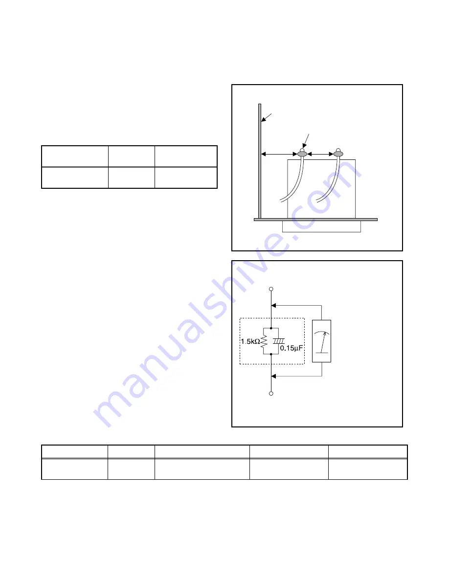
Insert load Z between B (earth ground, power cord plug 
prongs) and exposed accessible parts. Use an AC 
voltmeter to measure across both terminals of load Z. 
See Fig. 2 and following table.

Table 2: Leakage current ratings for selected areas

Note:

  This table is unofficial and for reference only. Be sure to confirm the precise values.

AC Line Voltage

Region

Clearance 

Distance (d), (d’)

110 to 130 V

U.S.A. or 

Canada

 3.2 mm 

(0.126 inches)

AC Line Voltage

Region

Load Z

Leakage Current (i)

Earth Ground (B) to:

110 to 130 V

U.S.A. or 

Canada

0.15 

µ

F CAP. & 1.5 k


RES. Connected in parallel

 0.5 mA rms

Exposed accessible 

parts

Chassis or Secondary Conductor

d

d'

Primary Circuit Terminals

Fig. 1

AC Voltmeter 
(High Impedance)

Exposed Accessible Part

B

Earth Ground 
Power Cord Plug Prongs

Z

Fig. 2

Summary of Contents for EWL2005

Page 1: ...SERVICE MANUAL 20 COLOR LCD TELEVISION EWL2005 ...

Page 2: ... service might be done or of the possible hazardous consequences of each way Consequently Funai has not undertaken any such broad evaluation Accordingly a servicer who uses a service procedure or tool which is not recommended by Funai must first use all precautions thoroughly so that neither his safety nor the safe operation of the equipment will be jeopardized by the service method selected TABLE...

Page 3: ...Unit Nominal Limit 1 Intermediate Freq Picture Sound MHz MHz 45 75 41 25 2 Color Killer Sens CH 2 CH 10 CH 55 dBµV dBµV dBµV 15 15 15 20 20 20 3 AFT Pull In Range 10 mV input MHz 2 1 0 7 Description Condition Unit Nominal Limit 1 Number of Pixels Horizontal Vertical pixels pixels 640 3 480 2 Brightness cd m2 500 3 Response Time msec 16 4 Support Color 26 mil 6 bit 5 Viewing Angle Horizontal Vertic...

Page 4: ...om any AC source connect an electrical jumper across the two AC plug prongs Place the instrument AC switch in the on position Connect one lead of an ohmmeter to the AC plug prongs tied together and touch the other ohmmeter lead in turn to each tuner antenna input exposed terminal screw and if applicable to the coaxial connector If the measured resistance is less than 1 0 megohm or greater than 5 2...

Page 5: ... is not isolated from the AC power line The two ground systems are electrically separated by insulation material that must not be defeated or altered 5 Observe original lead dress Take extra care to assure correct lead dress in the following areas a near sharp edges b near thermally hot parts be sure that leads and components do not touch thermally hot parts c the AC supply d high voltage and e an...

Page 6: ...ts H When a power cord has been replaced check that 5 6 kg of force in any direction will not loosen it I Also check areas surrounding repaired locations J Use care that foreign objects screws solder droplets etc do not remain inside the set K Crimp type wire connector The power transformer uses crimp type connectors which connect the power cord and the primary side of the transformer When replaci...

Page 7: ...ed accessible parts RF terminals antenna terminals video and audio input and output terminals microphone jacks earphone jacks etc is lower than or equal to the specified value in the table below Measuring Method Power ON Insert load Z between B earth ground power cord plug prongs and exposed accessible parts Use an AC voltmeter to measure across both terminals of load Z See Fig 2 and following tab...

Page 8: ...the Flat Pack IC about 5 to 6 seconds Fig S 1 1 2 Remove the flat pack IC with tweezers while applying the hot air 3 Bottom of the flat pack IC is fixed with glue to the CBA when removing entire flat pack IC first apply soldering iron to center of the flat pack IC and heat up Then remove glue will be melted Fig S 1 6 4 Release the flat pack IC from the CBA using tweezers Fig S 1 6 CAUTION 1 The Fl...

Page 9: ...y one using a sharp pin or wire to which solder will not adhere iron wire When heating the pins use a fine tip soldering iron or a hot air desoldering machine Fig S 1 4 3 Bottom of the flat pack IC is fixed with glue to the CBA when removing entire flat pack IC first apply soldering iron to center of the flat pack IC and heat up Then remove glue will be melted Fig S 1 6 4 Release the flat pack IC ...

Page 10: ...s Fig S 1 6 Note When using a soldering iron care must be taken to ensure that the flat pack IC is not being held by glue When the flat pack IC is removed from the CBA handle it gently because it may be damaged if force is applied 2 Installation 1 Using desoldering braid remove the solder from the foil of each pin of the flat pack IC on the CBA so you can install a replacement flat pack IC more ea...

Page 11: ...d to remove any static electricity that may be charged on the body 2 Ground for Workbench Be sure to place a conductive sheet or copper plate with proper grounding 1 MΩ on the workbench or other surface where the semi conductors are to be placed Because the static electricity charge on clothing will not escape through the body grounding band be careful to avoid contacting semi conductors with your...

Page 12: ...Spring L Locking Tab S Screw CN Connector Unhook Unlock Release Unplug or Desolder e g 2 S 2 two Screws S 2 2 L 2 two Locking Tabs L 2 5 Refer to the following Reference Notes in the Table Step Loc No Part Removal Fig No Remove Unhook Unlock Release Unplug Unclamp Desolder Note 1 Rear Cabinet D1 9 S 1 2 S 2 2 Jack Holder D2 3 S 3 S 4 3 Inverter CBA D2 D3 5 S 5 CN450 CN460 CN490 CLN411 4 Main CBA D...

Page 13: ...ear Cabinet Fig D2 S 10 S 9 S 8 S 8 S 10 S 7 S 7 S 7 S 3 S 3 S 6 S 6 S 6 S 5 S 5 S 4 S 7 S 7 S 3 S 6 S 6 5 LCD Main CBA Liquid Crystal Panel Unit 7 IR Sensor CBA 4 Main CBA 3 Inverter CBA 2 Jack Holder 6 Function CBA 8 Speaker 8 Speaker 9 Front Cabinet ...

Page 14: ...01 Function CBA IR Sensor CBA Inverter CBA Main CBA LCD Main CBA Unit To Speaker To Speaker CN103A CN312 CN311 CN460 CN101B CN102B CN103B CLN411 CN411 CN490 CN450 CN105 To Liquid Crystal Panel To Liquid Crystal Panel Fig D3 CN104 CLN104 CLN105 CN111 CN113 CN112 ...

Page 15: ...te control unit Part No N0105UD or N0127UD Remove 3 Screws from the back lid Fig 1 1 2 Added J1 Jumper Wire to the remote control CBA Fig 1 2 How to set up the service mode Service mode 1 Use the service remote control unit 2 Turn the power on Use main power on the TV unit 3 Press SLEEP button on the service remote control unit Version of micro computer will be displayed on the LCD or display Ex 0...

Page 16: ...become the following 4 Press CH o p buttons on the remote control unit so that flash stops D2 BRT MENU 5 137 D2 CNT 180 D2 CLR R 70 D2 CLR B 66 D2 TNT 60 D2 SHR 28 D3 BRT MENU 6 144 D3 CNT 195 D3 CLR R 70 D3 CLR B 66 D3 TNT 60 D3 SHR 28 DR C D1 VOL p 4 138 D DR C D2 165 DB C D1 VOL p 6 138 D DB C D2 165 Item Button on the service remote control Data Value VCOM 110 VCOM 110 FLASH Go and Off ...

Page 17: ...he Service mode Press VOL p button on the remote control unit and select C D S 1 mode VIDEO2 Enter the Service mode Press VOL p button on the remote control unit and select C D S 2 mode 5 RF VIDEO1 When x value and y value are not within specification adjust DB C D1 or DR C D1 Refer to 1 Initial Setting Note DB C D1 or DR C D1 must be adjusted within 0 01 VIDEO2 When x value and y value are not wi...

Page 18: ...unit 2 To enter the service mode press POWER 2 7 1 and MUTE buttons on the remote control unit in that order within 5 seconds To cancel the service mode press POWER button on the remote control 3 To initialize the LCD television press DISPLAY button on the remote control unit 4 Confirm FF indication on the upper right of the screen ...

Page 19: ...F VIDEO BLOCK DIAGRAM TO AUDIO BLOCK DIAGRAM BACKLIGHT SW BACKLIGHT ADJ P ON H VOLUME AUDIO MUTE INPUT 0 INPUT 1 S SW SCL SDA TO LCD BACKLIGHT BLOCK DIAGRAM CN102B CN102A SDA 2 SCL 1 CN112 NO CONNECTION IC171 MEMORY SCL 6 SDA 5 7 WP Q131 3 3V 5V CONVERTER BUS OPEN 4 NO PART MOUNTED FOR CN112 23 BUS OPEN P ON H2 NU 14 10 16 P ON H2 12 P 25V ON P 25V ON TO POWER SUPPLY BLOCK DIAGRAM KEY SWITCH IR SE...

Page 20: ... Q32 SDA TO SYSTEM CONTROL BLOCK DIAGRAM SCL S SW C Y CN103A TO LCD BLOCK DIAGRAM CN103B VIDEO Y 5 VIDEO Pb Cb 3 VIDEO Pr Cr 1 3 IC781 INPUT SELECT 5 Q703 4 13 12 Q702 14 1 2 Q701 15 SW CONTROL 10 9 11 INPUT 0 INPUT 1 TO SYSTEM CONTROL BLOCK DIAGRAM Q707 Q708 Q704 Q705 Q706 TUNER UNIT BUFFER BUFFER BUFFER BUFFER BUFFER BUFFER WF7 WF8 WF9 WF10 WF11 WF12 CF31 IC31 IF SIGNAL PROCESS VIF AMP VIDEO DET...

Page 21: ...CEL L R FILTER L R SAP SW SAP FILTER I2C DECORDER SAP DEMOD SAP OUT FILTER 29 30 TO IF VIDEO BLOCK DIAGRAM TUNER TUNER L CH R CH 21 27 24 IC851 MTS SAP AUDIO SIGNAL PROCESS AUDIO1 L IN JK704 SIF JK705 AUDIO1 R IN JK709 AUDIO2 L IN JK710 AUDIO2 R IN OFFSET CANCEL 14 IC801 AUDIO AMP 7 VOLUME 11 AMP AMP MUTE STANDBY CONTROL 6 1 R CH L CH 2 Q802 Q803 5 RF JK801 HEADPHONE JACK SP801 SPEAKER R CH CN801 ...

Page 22: ...ER 4 2 ER 5 1 EG 0 50 EG 1 49 EG 2 48 EG 3 47 EG 4 46 EG 5 45 EB 0 43 EB 1 42 EB 2 41 EB 3 40 EB 4 39 EB 5 38 OFFEV 12 STV1 13 CLKV 14 HMS1 E 7 HMS1 0 13 STH1 42 POL 43 LP 44 CN311 170 60 52 74 169 166 165 164 163 162 161 157 156 155 154 153 152 148 147 146 145 138 137 136 135 130 129 128 127 126 125 118 117 116 115 114 113 108 107 101 105 106 144 139 172 173 174 A D VIDEO SIGNAL PROCESS LCD RGB S...

Page 23: ...DIAGRAM TP401 21V Q633 CN101B PANEL 3 3V PANEL 10 8V PANEL 25V PANEL 6V LCD MAIN CBA UNIT P 25V ON AL 5V CN102B TO SYSTEM CONTROL BLOCK DIAGRAM TO LCD BACKLIGHT BLOCK DIAGRAM CAUTION Fixed voltage or Auto voltage selectable power supply circuit is used in this unit If Main Fuse F601 is blown check to see that all components in the power supply circuit are not defective before you connect the AC pl...

Page 24: ... 1 16 8V REG OUTPUT LOGIC1 OUTPUT LOGIC2 LOGIC OVER VOLTAGE PROTECT SLOW START OSC PWM2 PWM1 STANDBY MODE SW 4 5 7 OVER VOLTAGE PROTECTOR Q451 452 OVER VOLTAGE PROTECTOR Q454 455 7 6 9 8 1 2 13 14 T490 CN490 OVER VOLTAGE PROTECTOR Q491 492 1 2 1 2 T460 CN460 OVER VOLTAGE PROTECTOR Q461 462 10 IC402 OP AMP TO SYSTEM CONTROL BLOCK DIAGRAM AL 21V 9 7 3 1 6 4 2 5 10 8 9 7 3 1 6 4 2 5 10 8 9 7 3 1 6 4 ...

Page 25: ...ings for ordering The correct part number is shown in the parts list and may be slightly different or amended since these drawings were prepared 2 All resistance values are indicated in ohms K 103 M 106 3 Resistor wattages are 1 4W or 1 6W unless otherwise specified 4 All capacitance values are indicated in µF P 10 6 µF 5 All voltages are DC voltages unless otherwise specified Note of Capacitors M...

Page 26: ... the drawings were prepared 2 To maintain original function and reliability of repaired units use only original replacement parts which are listed with their part numbers in the parts list section of the service manual 4 Voltage indications on the schematics are as shown below Plug the TV power cord into a standard AC outlet 5 How to read converged lines 6 Test Point Information 2 3 1 5 0 3 0 5 0 ...

Page 27: ...MAIN 1 4 Ref No Position IC531 D 4 IC533 E 3 IC671 E 2 IC672 E 2 Q501 C 4 Q502 C 4 Q503 B 3 Q505 C 3 Q509 C 3 Q510 B 2 Q511 C 3 Q512 C 2 Q513 C 2 Q531 D 3 Q633 E 1 CN411 F 4 CN101A A 4 CN102A A 3 TP401 E 4 ICS TRANSISTORS TEST POINT CONNECTORS ...

Page 28: ...8 4 L3202SCM2 Main 2 4 Schematic Diagram MAIN 2 4 Ref No Position IC31 I 1 IC851 H 3 IC852 J 4 Q32 J 2 CN113 G 1 ICS TRANSISTOR CONNECTOR ...

Page 29: ...ematic Diagram L3202SCM3 MAIN 3 4 Ref No Position IC781 P 3 IC801 N 2 Q701 N 3 Q702 N 3 Q703 N 3 Q704 P 1 Q705 O 1 Q706 P 1 Q707 P 2 Q708 P 2 Q802 O 1 Q803 N 1 CN801 M 4 CN802 M 3 CN103A M 2 CONNECTORS ICS TRANSISTORS ...

Page 30: ...ll components in the power supply circuit are not defective before you connect the AC plug to the AC power supply Otherwise it may cause some components in the power supply circuit to fail NOTE The voltage for parts in hot circuit is measured using hot GND as a common terminal For continued protection against risk of fire replace only with same type 4 A 125V fuse CAUTION ATTENTION Utiliser un fusi...

Page 31: ...m INVERTER Ref No Position IC401 A 3 IC402 E 3 Q403 B 1 Q411 B 3 Q412 B 3 Q421 B 4 Q426 B 3 Q433 B 2 Q451 E 4 Q452 D 4 Q454 D 3 Q455 D 3 Q461 E 2 Q462 D 2 Q491 D 3 Q492 D 3 CLN411 A 1 CN450 F 4 CN460 F 2 CN490 F 4 ICS TRANSISTORS CONNECTORS ...

Page 32: ...8 8 L3202SCF Function Schematic Diagram ...

Page 33: ...8 9 L3202SCIR IR Sensor Schematic Diagram ...

Page 34: ...8 10 L3202SCL1 LCD Main 1 2 Schematic Diagram LCD MAIN 1 2 Ref No Position IC333 B 3 Q301 D 1 CN104 A 3 CN105 A 2 CN111 A 2 CN211 F 4 CN311 F 4 CN102B A 4 CONNECTORS TRANSISTOR TRANSISTOR ...

Page 35: ...2 LCD Main 2 2 Schematic Diagram LCD MAIN 2 2 Ref No Position IC151 I 3 IC171 J 3 IC191 H 2 IC192 H 1 IC193 H 2 IC201 J 1 Q131 I 4 Q201 J 1 CN112 L 4 CN312 L 3 CN101B L 4 CN103B G 2 TRANSISTOR CONNECTORS TRANSISTOR ...

Page 36: ... that all components in the power supply circuit are not defective before you connect the AC plug to the AC power supply Otherwise it may cause some components in the power supply circuit to fail NOTE The voltage for parts in hot circuit is measured using hot GND as a common terminal Because a hot chassis ground is present in the power supply circuit an isolation transformer must be used Also in o...

Page 37: ... power supply circuit to fail NOTE The voltage for parts in hot circuit is measured using hot GND as a common terminal Because a hot chassis ground is present in the power supply circuit an isolation transformer must be used Also in order to have the ability to increase the input slowly when troubleshooting this type power supply circuit a variable isolation transformer is required MAIN CBA Ref No...

Page 38: ...8 14 BL3100F01011 3 Function CBA Top View Function CBA Bottom View IR Sensor CBA Top Bottom View BL3100F01021 2 BL3100F01021 2 ...

Page 39: ...8 15 Inveretr CBA Top View Inverter CBA Bottom View BL3100F01021 1 ...

Page 40: ...chematic Diagram 1DIV 1 0V 20ns R365 WF2 R202 WF3 1DIV 200mV 20 s Pin 11 of CN103A WF7 1DIV 200mV 20 s Pin 9 of CN103A WF8 1DIV 100mV 400 s Pin 14 of IC801 WF6 1DIV 1 0V 10 s R201 WF4 1DIV 200mV 20 s Pin 7 of CN103A WF9 1DIV 200mV 20 s Q704 Emitter WF10 1DIV 200mV 20 s Q705 Emitter WF11 1DIV 200mV 20 s Q706 Emitter WF12 CLKH CLKV POL LP STH1 AUDIO CVBS S VIDEO Y S VIDEO C VIDEO Y VIDEO Pb Cb VIDEO...

Page 41: ...2 CN105 REMOTE AL 5V GND P ON H INVERTER CBA BACK LIGHT CN450 2 1 BACK LIGHT CN490 2 1 CN311 1 3 2 5 4 7 6 8 9 10 13 12 11 14 15 17 16 19 18 21 20 22 23 24 27 26 25 28 29 30 GND CLKH GND GND HMS1 E ER 0 ER 1 ER 2 ER 3 ER 4 ER 5 GND HMS1 0 GND OB 5 OB 4 OB 3 OB 2 OB 1 OB 0 GND OG 5 OG 4 OG 3 OG 2 OG 1 OG 0 GND OR 5 OR 4 33 32 31 34 35 37 36 39 38 41 40 42 43 44 45 OR 3 OR 2 OR 1 OR 0 GND GND VDDD 3...

Page 42: ...arts List for parts with this mark Main CBA AC601 B5 B5 B8 B8 A1 A3 A2 L7 L7 L1 L7 L1 L1 L1 L3 B10 B6 B7 L3 L3 L3 L3 L3 L17 L17 A6 S5 A5 L2 L2 L6 L2 L2 L2 L10 A5 A4 A10 L3 L4 L9 B3 B4 L1 L1 L3 A9 L3 L3 Inverter CBA LCD Main CBA Liquid Crystal Panel Unit Function CBA IR Sensor CBA ...

Page 43: ...11 2 L3202PEX Packing S1 FRONT S2 S5 S4 Tape Tape Packing Tape Packing Tape Packing Tape S3 X1 X4 X3 Some Ref Numbers are not in sequence X2 S6 ...

Page 44: ...CLOTH 10X30XT0 5 B5900UA 0EM404486 B8 CLOTH 10X150XT1 0 1EM421092 CLN801 SPEAKER WIRE ASSEMBLY WX1L3100 001 WX1L3100 001 CLN802 SPEAKER WIRE ASSEMBLY WX1L3100 001 WX1L3100 001 L1 SCREW P TIGHT 3X14 WASHER HEAD GCMP3140 L2 SCREW P TIGHT 3X12 BIND HEAD GBMP3120 L3 SCREW S TIGHT M3X8 BIND HEAD GBMS3080 L6 DOUBLE SEMS SCREW M4X9 L0130UA 0EM408146 L7 SCREW ASSEMBLED 12 M3X12 0EM406746 L9 SCREW P TIGHT ...

Page 45: ...CTROLYTIC CAP 220µF 16V M H7 CE1CMASSL221 C504 ELECTROLYTIC CAP 100µF 10V M H7 CE1AMASSL101 C505 CHIP CERAMIC CAP 1608 B K 0 01µF 50V CHD1JK30B103 C506 CHIP CERAMIC CAP 1608 B K 0 01µF 50V CHD1JK30B103 C507 CHIP CERAMIC CAP 1608 B K 0 01µF 50V CHD1JK30B103 C508 CHIP CERAMIC CAP 1608 B K 0 01µF 50V CHD1JK30B103 C515 CHIP CERAMIC CAP 1608 B K 0 01µF 50V CHD1JK30B103 C531 ELECTROLYTIC CAP 330µF 50V M...

Page 46: ...08 B K 0 01µF 50V CHD1JK30B103 C863 ELECTROLYTIC CAP 2 2µF 50V M H7 CE1JMASSL2R2 C864 CHIP CERAMIC CAP 1608 B K 0 022µF 50V CHD1JK30B223 C865 CHIP CERAMIC CAP 1608 B K 0 1µF 50V CHD1JK30B104 C866 CHIP CERAMIC CAP F Z 2 2µF 10V CHD1AZ30F225 C867 CHIP CERAMIC CAP F Z 2 2µF 10V CHD1AZ30F225 C868 CHIP CERAMIC CAP B K 1µF 16V CHD1CK30B105 C869 CHIP CERAMIC CAP 1608 B K 0 022µF 50V CHD1JK30B223 Ref No D...

Page 47: ...NSISTOR 2SA1175 F QQSF02SA1175 RESISTORS R11 CHIP RES 1608 1 10W J 100 Ω RRXAJR5Z0101 R12 CHIP RES 1608 1 10W J 100 Ω RRXAJR5Z0101 R13 INDUCTOR 0 47µH J 26T LLAXJATTUR47 R15 CHIP RES 1608 1 10W J 4 7k Ω RRXAJR5Z0472 R21 CHIP RES 1608 1 10W J 68k Ω RRXAJR5Z0683 R23 CHIP RES 1608 1 10W J 2 2k Ω RRXAJR5Z0222 R24 CHIP RES 1608 1 10W J 100k Ω RRXAJR5Z0104 R34 CHIP RES 1608 1 10W 0 Ω RRXAZR5Z0000 R36 CA...

Page 48: ...47 CHIP RES 1608 1 10W J 39k Ω RRXAJR5Z0393 Ref No Description Part No R748 CHIP RES 1608 1 10W J 33k Ω RRXAJR5Z0333 R749 CHIP RES 1608 1 10W J 39k Ω RRXAJR5Z0393 R752 CHIP RES 1608 1 10W J 18k Ω RRXAJR5Z0183 R755 CHIP RES 1608 1 10W J 18k Ω RRXAJR5Z0183 R756 CHIP RES 1608 1 10W J 10k Ω RRXAJR5Z0103 R757 CHIP RES 1608 1 10W J 47k Ω RRXAJR5Z0473 R758 CHIP RES 1608 1 10W J 47k Ω RRXAJR5Z0473 R759 CH...

Page 49: ...ollowing 1ESA10623 INVERTER CBA FUNCTION CBA Ref No Description Part No INVERTER CBA Consists of the following CAPACITORS C401 ELECTROLYTIC CAP 47µF 35V M H7 CE1GMASSL470 C402 CHIP CERAMIC CAP 1608 B K 0 1µF 50V CHD1JK30B104 C403 ELECTROLYTIC CAP 100µF 16V M H7 CE1CMASSL101 C404 CHIP CERAMIC CAP 1608 B K 0 01µF 50V CHD1JK30B103 C405 CHIP CERAMIC CAP 1608 B K 0 047µF 50V CHD1JK30B473 C406 CHIP CERA...

Page 50: ...T106 Q QQ1Q02SC4081 Ref No Description Part No Q491 TRANSISTOR 2SC4081 T106 Q QQ1Q02SC4081 Q492 TRANSISTOR 2SC4081 T106 Q QQ1Q02SC4081 RESISTORS R402 CHIP RES 1608 1 10W J 10k Ω RRXAJR5Z0103 R404 CHIP RES 1608 1 10W J 5 1k Ω RRXAJR5Z0512 R405 CARBON RES 1 4W J 1k Ω RCX4JATZ0102 R406 CARBON RES 1 4W J 1k Ω RCX4JATZ0102 R407 METAL RESISITOR 2W J 2 2k Ω RN02222ZU001 R408 METAL RESISITOR 2W J 2 2k Ω R...

Page 51: ...ists of the following CAPACITOR C61 CHIP CERAMIC CAP 1608 B K 0 01µF 50V CHD1JK30B103 RESISTORS R61 CHIP RES 1608 1 10W J 10k Ω RRXAJR5Z0103 R62 CHIP RES 1608 1 10W J 47 Ω RRXAJR5Z0470 R63 CHIP RES 1608 1 10W J 1 5k Ω RRXAJR5Z0152 R64 CHIP RES 1608 1 10W J 1 5k Ω RRXAJR5Z0152 R65 CHIP RES 1608 1 10W J 2 2k Ω RRXAJR5Z0222 R66 CHIP RES 1608 1 10W J 2 7k Ω RRXAJR5Z0272 R67 CHIP RES 1608 1 10W J 4 7k ...

Page 52: ...EWL2005 L3202UC 2005 04 06 ...

Reviews: