background image

8-8

L2601SCF

 Function Schematic Diagram

Summary of Contents for EWL20S5

Page 1: ...s different from the original EWL20S5 and the EWL20S5 version A model For EWL20S5 version B model a suffix B is printed on the rating label on the back of the unit Refer to the rating label illustration at right LCD COLOR TV Rating Label Suffix B 20 COLOR LCD TELEVISION EWL20S5 ...

Page 2: ... service might be done or of the possible hazardous consequences of each way Consequently Funai has not undertaken any such broad evaluation Accordingly a servicer who uses a service procedure or tool which is not recommended by Funai must first use all precautions thoroughly so that neither his safety nor the safe operation of the equipment will be jeopardized by the service method selected TABLE...

Page 3: ...t Nominal Limit 1 Intermediate Freq Picture Sound MHz MHz 45 75 41 25 2 Color Killer Sens CH 2 CH 10 CH 55 dBµV dBµV dBµV 15 15 15 20 20 20 3 AFT Pull In Range 10 mV input MHz 2 1 0 7 Description Condition Unit Nominal Limit 1 Number of Pixels Horizontal Vertical pixels pixels 640 3 480 2 Brightness cd m2 500 3 Response Time msec 16 4 Support Color 26 mil 6 bit 5 Viewing Angle Horizontal Vertical ...

Page 4: ...om any AC source connect an electrical jumper across the two AC plug prongs Place the instrument AC switch in the on position Connect one lead of an ohmmeter to the AC plug prongs tied together and touch the other ohmmeter lead in turn to each tuner antenna input exposed terminal screw and if applicable to the coaxial connector If the measured resistance is less than 1 0 megohm or greater than 5 2...

Page 5: ... is not isolated from the AC power line The two ground systems are electrically separated by insulation material that must not be defeated or altered 5 Observe original lead dress Take extra care to assure correct lead dress in the following areas a near sharp edges b near thermally hot parts be sure that leads and components do not touch thermally hot parts c the AC supply d high voltage and e an...

Page 6: ...ts H When a power cord has been replaced check that 5 6 kg of force in any direction will not loosen it I Also check areas surrounding repaired locations J Use care that foreign objects screws solder droplets etc do not remain inside the set K Crimp type wire connector The power transformer uses crimp type connectors which connect the power cord and the primary side of the transformer When replaci...

Page 7: ...exposed accessible parts RF terminals antenna terminals video and audio input and output terminals microphone jacks earphone jacks etc is lower than or equal to the specified value in the table below Measuring Method Power ON Insert load Z between B earth ground power cord plug prongs and exposed accessible parts Use an AC voltmeter to measure across both terminals of load Z See Fig 2 and followin...

Page 8: ...the Flat Pack IC about 5 to 6 seconds Fig S 1 1 2 Remove the flat pack IC with tweezers while applying the hot air 3 Bottom of the flat pack IC is fixed with glue to the CBA when removing entire flat pack IC first apply soldering iron to center of the flat pack IC and heat up Then remove glue will be melted Fig S 1 6 4 Release the flat pack IC from the CBA using tweezers Fig S 1 6 CAUTION 1 The Fl...

Page 9: ...y one using a sharp pin or wire to which solder will not adhere iron wire When heating the pins use a fine tip soldering iron or a hot air desoldering machine Fig S 1 4 3 Bottom of the flat pack IC is fixed with glue to the CBA when removing entire flat pack IC first apply soldering iron to center of the flat pack IC and heat up Then remove glue will be melted Fig S 1 6 4 Release the flat pack IC ...

Page 10: ...s Fig S 1 6 Note When using a soldering iron care must be taken to ensure that the flat pack IC is not being held by glue When the flat pack IC is removed from the CBA handle it gently because it may be damaged if force is applied 2 Installation 1 Using desoldering braid remove the solder from the foil of each pin of the flat pack IC on the CBA so you can install a replacement flat pack IC more ea...

Page 11: ...d to remove any static electricity that may be charged on the body 2 Ground for Workbench Be sure to place a conductive sheet or copper plate with proper grounding 1 MΩ on the workbench or other surface where the semi conductors are to be placed Because the static electricity charge on clothing will not escape through the body grounding band be careful to avoid contacting semi conductors with your...

Page 12: ...nclamped or desoldered P Spring L Locking Tab S Screw CN Connector Unhook Unlock Release Unplug or Desolder e g 2 S 2 two Screws S 2 2 L 2 two Locking Tabs L 2 5 Refer to the following Reference Notes in the Table Step Loc No Part Removal Fig No Remove Unhook Unlock Release Unplug Unclamp Desolder Note 1 Rear Cabinet D1 12 S 1 S 2 4 S 3 2 Jack Holder D2 3 S 4 S 5 3 Inverter CBA D2 D3 4 S 6 CN301 C...

Page 13: ... 2 S 1 S 1 S 1 Fig D2 S 9 S 9 S 11 S 11 Speaker Holders S 10 S 8 S 8 S 8 S 8 S 8 S 8 S 6 S 6 S 5 S 4 S 7 S 7 S 7 S 7 S 4 S 4 7 IR Sensor CBA 4 Main CBA 3 Inverter CBA 2 Jack Holder 6 Function CBA 8 Speaker 8 Speaker 9 Front Cabinet Speaker Holders 5 LCD Module ...

Page 14: ...Cable Wiring Diagram Fig D3 IR Sensor CBA To LCD Module CN310 To Speaker Function CBA CLN104 CN801 To Speaker CN1202 CLN105 CN1207 CN1206 CN1205 To LCD Module Main CBA CN404 CN304 Inverter CBA CN301 CN302 CN303 CN1201 ...

Page 15: ...ontrol unit Part No N0105UD or N0127UD Remove 3 Screws from the back lid Fig 1 1 2 Added J1 Jumper Wire to the remote control CBA Fig 1 2 How to set up the service mode Service mode 1 Use the service remote control unit 2 Turn the power on Use main power on the TV unit 3 Press SLEEP button on the service remote control unit Version of micro computer will be displayed on the LCD or display Ex 0008G...

Page 16: ...come the following 4 Press CH o p buttons on the remote control unit so that flash stops D2 BRT MENU 5 133 D2 CNT 140 D2 CLR R 74 D2 CLR B 74 D2 TNT 128 D2 SHR 112 D3 BRT MENU 6 126 D3 CNT 138 D3 CLR R 64 D3 CLR B 64 D3 TNT 128 D3 SHR 112 DR C D1 VOL p 4 176 C DR C D2 157 DB C D1 VOL p 6 175 C DB C D2 152 Item Button on the service remote control Data Value VCOM 110 VCOM 110 FLASH Go and Off ...

Page 17: ...r the Service mode Press VOL p button on the remote control unit and select C D 1 mode VIDEO2 Enter the Service mode Press VOL p button on the remote control unit and select C D 2 mode 5 RF VIDEO1 When x value and y value are not within specification adjust DB C D1 or DR C D1 Refer to 1 Initial Setting Note DB C D1 or DR C D1 must be adjusted within 0 01 VIDEO2 When x value and y value are not wit...

Page 18: ...ain power on the TV unit 2 To enter the service mode press SLEEP button on the service remote control unit To cancel the service mode press POWER button on the remote control 3 To initialize the LCD television press DISPLAY button on the remote control unit 4 Confirm FF indication on the upper right of the screen ...

Page 19: ...PUT 1 S SW SCL SDA 32 11 13 35 12 14 36 TO POWER SUPPLY BLOCK DIAGRAM TO IF VIDEO BLOCK DIAGRAM TO AUDIO BLOCK DIAGRAM BACKLIGHT ADJ P ON H VOLUME AUDIO MUTE INPUT 0 INPUT 1 S SW SCL SDA SDA 2 SCL 1 CN1209 NO CONNECTION IC1205 MEMORY SCL 6 SDA 5 7 WP Q1204 3 3V 5V CONVERTER BUS OPEN 4 NO PART MOUNTED FOR CN1209 33 BUS OPEN 27 P 25V ON IR SENSOR CBA CLN105 REMOTE SENSOR RCV91 CN1202 REMOTE 3 3 6 AF...

Page 20: ...O Pr Cr IN JK703 VIDEO1 IN JK701 S VIDEO IN SDA TO SYSTEM CONTROL BLOCK DIAGRAM SCL S SW C Y 3 IC781 INPUT SELECT 5 4 13 12 14 1 2 15 SW CONTROL 10 9 11 INPUT 0 INPUT 1 TO SYSTEM CONTROL BLOCK DIAGRAM Q707 Q708 TUNER UNIT CF31 IC31 IF SIGNAL PROCESS VIF AMP VIDEO DET VCO 4 5MHz FILTER RF AGC AMP SIF AMP 16 13 18 17 4 7 8 1 XTAL IN 14 TO SYSTEM CONTROL BLOCK DIAGRAM AFT IN 5 SIF TRAP 11 FSC IF AGC ...

Page 21: ...R FILTER L R SAP SW SAP FILTER I2C DECORDER SAP DEMOD SAP OUT FILTER 29 30 TO IF VIDEO BLOCK DIAGRAM TUNER TUNER L CH R CH 21 27 24 IC851 MTS SAP AUDIO SIGNAL PROCESS AUDIO1 L IN JK704 SIF JK705 AUDIO1 R IN JK709 AUDIO2 L IN JK710 AUDIO2 R IN OFFSET CANCEL 14 IC801 AUDIO AMP 7 VOLUME 11 AMP AMP MUTE STANDBY CONTROL 6 1 R CH L CH 2 Q802 JK801 HEADPHONE JACK SP801 SPEAKER R CH CN801 SP R 1 GND 2 SP8...

Page 22: ...G 4 17 EG 5 16 EB 0 14 EB 1 13 EB 2 12 EB 3 11 EB 4 10 EB 5 9 OFFEV 5 STV1 6 CLKV 7 ODDINV 3 VCOM 18 VCOM 19 EVENINV 1 STH1 26 POL 27 LP 28 CN1206 CN1207 151 62 57 77 150 146 145 144 143 142 141 140 136 135 134 133 132 131 130 129 128 118 117 116 115 114 113 112 111 110 109 108 105 104 103 95 94 93 92 86 90 91 127 124 153 154 155 A D VIDEO SIGNAL PROCESS LCD RGB SIGNAL PROCESS R B G Y Pb Cb Pr Cr ...

Page 23: ...AM TO LCD BACKLIGHT BLOCK DIAGRAM D647 SHUNT REG IC1605 5V REG IC1606 5V REG Q402 Q401 Q403 IC1603 1 5V REG IC1602 3 3V REG VT 33V D505 SHUNT REG TO LCD MODULE CAUTION Fixed voltage or Auto voltage selectable power supply circuit is used in this unit If Main Fuse F601 is blown check to see that all components in the power supply circuit are not defective before you connect the AC plug to the AC po...

Page 24: ...NV 22V 9 7 3 5 2 6 1 4 10 8 TO POWER SUPPLY BLOCK DIAGRAM MAIN CBA AL 21V 7 7 CN404 CN304 AL 21V 6 6 AL 21V 5 5 AL 21V 4 4 AL 21V 8 8 AL 21V 9 9 CURRENT CONTROL SWITCH Q341 Q344 T302 OVER VOLTAGE PROTECTOR Q342 343 9 7 3 5 2 6 1 4 10 8 CURRENT CONTROL SWITCH Q361 Q364 T303 OVER VOLTAGE PROTECTOR Q362 363 9 7 3 5 2 6 1 4 10 8 OVER VOLTAGE PROTECTOR Q304 Q306 10V REG OVER CURERENT PROTECTOR Q325 Q30...

Page 25: ...ings for ordering The correct part number is shown in the parts list and may be slightly different or amended since these drawings were prepared 2 All resistance values are indicated in ohms K 103 M 106 3 Resistor wattages are 1 4W or 1 6W unless otherwise specified 4 All capacitance values are indicated in µF P 10 6 µF 5 All voltages are DC voltages unless otherwise specified Note of Capacitors M...

Page 26: ...mended since the drawings were prepared 2 To maintain original function and reliability of repaired units use only original replacement parts which are listed with their part numbers in the parts list section of the service manual 4 Voltage indications on the schematics are as shown below Plug the TV power cord into a standard AC outlet 5 How to read converged lines 6 Test Point Information 2 3 1 ...

Page 27: ...8 3 Main 1 5 Schematic Diagram L2601SCM1 ...

Page 28: ...8 4 L2601SCM2 Main 2 5 Schematic Diagram ...

Page 29: ...8 5 Main 3 5 Schematic Diagram L2601SCM3 ...

Page 30: ...8 6 L2601SCM4 Main 4 5 Schematic Diagram ...

Page 31: ...circuit are not defective before you connect the AC plug to the AC power supply Otherwise it may cause some components in the power supply circuit to fail NOTE The voltage for parts in hot circuit is measured using hot GND as a common terminal For continued protection against risk of fire replace only with same type 4 A 125V fuse CAUTION ATTENTION Utiliser un fusible de rechange de même type de 4A...

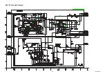
Page 32: ...8 8 L2601SCF Function Schematic Diagram ...

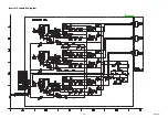
Page 33: ...8 9 L2601SCIR IR Sensor Schematic Diagram ...

Page 34: ...8 10 L2601SCI Inverter Schematic Diagram ...

Page 35: ...er supply Otherwise it may cause some components in the power supply circuit to fail For continued protection against risk of fire replace only with same type 4 A 125V fuse CAUTION ATTENTION Utiliser un fusible de rechange de même type de 4A 125V 4A 125V NOTE The voltage for parts in hot circuit is measured using hot GND as a common terminal Because a hot chassis ground is present in the power sup...

Page 36: ... used in this unit If Main Fuse F601 is blown check to see that all components in the power supply circuit are not defective before you connect the AC plug to the AC power supply Otherwise it may cause some components in the power supply circuit to fail NOTE The voltage for parts in hot circuit is measured using hot GND as a common terminal Because a hot chassis ground is present in the power supp...

Page 37: ...8 13 Function CBA Top View Function CBA Bottom View BL2601F01031 1 IR Sensor CBA Top View IR Sensor CBA Bottom View BL2601F01031 2 ...

Page 38: ...8 14 Inverter CBA Top View BL2500F01021 Inverter CBA Bottom View ...

Page 39: ...ram 1DIV 1 0V 20ns Pin 7 of CN1205 WF2 Pin 27 of CN1206 WF3 1DIV 200mV 20 s Pin 70 of IC1202 WF7 1DIV 200mV 20 s Pin 75 of IC1202 WF8 1DIV 100mV 400 s Pin 14 of IC801 WF6 1DIV 1 0V 10 s Pin 28 of CN1206 WF4 1DIV 200mV 20 s Pin 52 of IC1202 WF9 1DIV 200mV 20 s Pin 77 of IC1202 WF10 1DIV 200mV 20 s Pin 57 of IC1202 WF11 1DIV 200mV 20 s Pin 62 of IC1202 WF12 CLKH CLKV POL LP STH1 AUDIO CVBS S VIDEO Y...

Page 40: ...GND PANEL 25V NU GND CN1205 1 3 2 5 4 7 6 8 9 10 13 12 11 14 15 17 16 19 18 21 20 22 23 24 27 26 25 28 EB 3 EB 4 EB 5 GND CLKV STV1 OFFEV GND GND GND GND EB 2 EB 1 EB 0 GND EG 5 EG 4 EG 3 EG 2 EG 1 EG 0 GND ER 5 ER 4 ER 3 ER 2 ER 1 ER 0 CN404 CN304 1 3 2 5 4 7 6 8 9 10 13 12 11 14 GND GND 22V 22V 22V 22V 22V 22V PROTECT 1 SP L SP GND GND GND GND GND CN1206 1 3 2 5 4 7 6 8 9 10 13 12 11 14 15 17 16...

Page 41: ...CD1 L9 L14 L14 L14 L14 L16 L16 L14 L14 A9 L9 L23 L9 L9 L9 L9 L9 L9 A4 B3 B12 B21 B21 B21 L14 L22 S5 A8 L19 A10 L30 L9 L9 L22 L22 L22 A11 B14 L22 A7 L22 L22 B14 CLN801 SP801 CLN802 SP802 CLN320 See Electrical Parts List for parts with this mark Main CBA AC601 Inverter CBA Function CBA B22 IR Sensor CBA ...

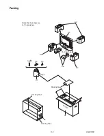
Page 42: ...11 2 L2601PEX Packing S1 FRONT S2 S5 S4 Tape Packing Tape Packing Tape Packing Tape S3 S3 S6 X1 X5 X3 Some Ref Numbers are not in sequence X2 Packing Tape ...

Page 43: ...LOTH 10X180XT0 5 L0336JG 0EM408827 CL1205 WIRE ASSEMBLY 28PIN 28PIN 92MM WHITE WX1L2600 001 CL1206 WIRE ASSEMBLY 28PIN 28PIN 92MM WHITE WX1L2600 001 CL1207 WIRE ASSEMBLY 28PIN 28PIN 92MM WHITE WX1L2600 001 CLN320 WIRE ASSEMBLY 1PIN 80MM BLACK WX1L2600 015 CLN801 WIRE ASSEMBLY 2PIN SPEAKER 2PIN 325MM WX1L2600 009 CLN802 WIRE ASSEMBLY 2PIN SPEAKER 2PIN 325MM WX1L2600 009 L9 SCREW P TIGHT 3X10 BIND H...

Page 44: ... 220µF 16V M CE1CMASDL221 C634 ELECTROLYTIC CAP 1000µF 10V M CE1AMASDL102 C635 ELECTROLYTIC CAP 470µF 25V M CE1EMASDL471 C636 ELECTROLYTIC CAP 220µF 50V M CE1JMASDL221 C637 ELECTROLYTIC CAP 470µF 16V M CE1CMASDL471 C638 CHIP CERAMIC CAP 1608 B K 0 22µF 16V CHD1CK30B224 C639 ELECTROLYTIC CAP 330µF 6 3V M CE0KMASDL331 C640 CHIP CERAMIC CAP 1608 B K 0 22µF 16V CHD1CK30B224 C641 SAFETY CAP 4700pF 250V...

Page 45: ...B104 C1248 ELECTROLYTIC CAP 47µF 16V M H7 CE1CMASSL470 C1249 ELECTROLYTIC CAP 47µF 16V M H7 CE1CMASSL470 C1250 CHIP CERAMIC CAP 1608 B K 0 01µF 50V CHD1JK30B103 C1251 CHIP CERAMIC CAP 1608 B K 0 01µF 50V CHD1JK30B103 C1253 CHIP CERAMIC CAP 1608 B K 0 22µF 16V CHD1CK30B224 C1254 CHIP CERAMIC CAP 1608 B K 0 22µF 16V CHD1CK30B224 C1255 CHIP CERAMIC CAP 1608 B K 0 22µF 16V CHD1CK30B224 Ref No Descript...

Page 46: ...M006 IC1202 IC DVP R8A01027A91FP RF0Z QSZAA0RHT116 IC1205 IC EEPROM 32K BR24L32F WE2 QSZBA0TRM067 IC1207 IC TL3472CDR NSZBA0TTY115 Ref No Description Part No IC1211 IC RESET BU4223G TR 5PIN QSZBA0TRM103 COILS L11 INDUCTOR 22µH K 5FT LLARKBSTU220 L12 INDUCTOR 22µH K 5FT LLARKBSTU220 L13 INDUCTOR 0 47µH J 26T LLAXJATTUR47 L21 INDUCTOR 100µH K 5FT LLARKBSTU101 L22 INDUCTOR 150µH J 26T LLAXJATTU151 L3...

Page 47: ...J 390 Ω RCX4JATZ0391 R659 CHIP RES 1 10W J 10k Ω RRXAJR5Z0103 R661 CARBON RES 1 4W J 470 Ω RCX4JATZ0471 Ref No Description Part No R663 CARBON RES 1 4W J 2 2 Ω RCX4JATZ02R2 R664 CARBON RES 1 4W J 2 2 Ω RCX4JATZ02R2 R665 CARBON RES 1 4W J 2 2 Ω RCX4JATZ02R2 R667 PCB JUMPER D0 6 P5 0 JW5 0T R669 CARBON RES 1 4W J 330 Ω RCX4JATZ0331 R670 CARBON RES 1 4W J 330 Ω RCX4JATZ0331 R671 CARBON RES 1 4W J 330...

Page 48: ... Ω RRXAJR5Z0153 R1277 CHIP RES 1608 1 10W 0 Ω RRXAZR5Z0000 R1278 CHIP RES 1 10W J 100 Ω RRXAJR5Z0101 Ref No Description Part No R1279 CHIP RES 1 10W J 75 Ω RRXAJR5Z0750 R1301 CHIP RES 1608 1 10W 0 Ω RRXAZR5Z0000 R1302 CHIP RES 1608 1 10W 0 Ω RRXAZR5Z0000 R1303 CHIP RES 1608 1 10W 0 Ω RRXAZR5Z0000 R1304 CHIP RES 1 10W J 56 Ω RRXAJR5Z0560 R1305 CHIP RES 1 10W J 56 Ω RRXAJR5Z0560 R1306 CHIP RES 1 10W...

Page 49: ...P 22µF 50V M CE1JMASDL220 C332 CHIP CERAMIC CAP 1608 B K 0 01µF 50V CHD1JK30B103 C341 CAP CHIP 5pF 3KV C XC CA3F5R05M016 C342 CHIP CERAMIC CAP 1608 B K 0 01µF 50V CHD1JK30B103 C343 CAP CHIP 5pF 3KV C XC CA3F5R05M016 C345 CHIP CERAMIC CAP 1608 B K 0 01µF 50V CHD1JK30B103 C346 ELECTROLYTIC CAP 10µF 50V M CE1JMASDL100 C347 CHIP CERAMIC CAP 1608 B K 0 01µF 50V CHD1JK30B103 C348 ELECTROLYTIC CAP 10µF 5...

Page 50: ...33 CHIP RES 1 10W J 10k Ω RRXAJR5Z0103 R334 CHIP RES 1 10W J 15k Ω RRXAJR5Z0153 R335 CHIP RES 1 10W J 2 2k Ω RRXAJR5Z0222 R336 CHIP RES 1 10W J 10k Ω RRXAJR5Z0103 R337 CHIP RES 1 10W J 10k Ω RRXAJR5Z0103 R341 CHIP RES 1 10W J 390 Ω RRXAJR5Z0391 R342 CHIP RES 1 10W J 390 Ω RRXAJR5Z0391 R343 CHIP RES 1 10W J 1k Ω RRXAJR5Z0102 Ref No Description Part No R344 CHIP RES 1 10W J 10k Ω RRXAJR5Z0103 R345 C...

Page 51: ...sists of the following LECTROLYTIC CAP 47µF 10V M H7 CE1AMASSL470 DIODE D91 LED L 53HT NP4Z000L53HT TRANSISTOR Q91 TRANSISTOR 2SC4081 T106 Q QQ1Q02SC4081 RESISTORS R91 CARBON RES 1 4W J 10k Ω RCX4JATZ0103 R92 CHIP RES 1 10W J 68 Ω RRXAJR5Z0680 R93 CARBON RES 1 4W J 68 Ω RCX4JATZ0680 R94 CARBON RES 1 4W J 150 Ω RCX4JATZ0151 R95 CHIP RES 1 10W J 150 Ω RRXAJR5Z0151 R96 CHIP RES 1 10W J 10k Ω RRXAJR5Z...

Page 52: ...EWL20S5 L2601UB 2006 05 29 ...

Page 53: ... not printed to the model number Refer to the Rating Label on the back of the unit to make sure model types This service manual is for the EWL20S5 C version model and shows only the differences between the EWL20S5 C version model and EWL20S5 B version model All other information is described in the service manual of the EWL20S5 B version model TM Rating Label Suffix C 20 COLOR LCD TELEVISION EWL20...

Page 54: ... 6 8k Ω RRXAFR5H6801 R516 CHIP RES 1 10W F 1 6k Ω RRXAFR5H1601 R522 CARBON RES 1 4W J 10 Ω RCX4JATZ0100 R523 CARBON RES 1 4W J 10 Ω RCX4JATZ0100 R524 CARBON RES 1 4W J 10 Ω RCX4JATZ0100 R525 CARBON RES 1 4W J 10 Ω RCX4JATZ0100 R1245 CHIP RES 1 10W F 470 Ω RRXAFR5H0471 R1246 CHIP RES 1 10W F 330 Ω RRXAFR5H3300 R1247 CHIP RES 1 10W F 470 Ω RRXAFR5H0471 R1251 CHIP RES 1 10W F 180 Ω RRXAFR5H1800 R1255...

Reviews: