background image

Endace Measurement Systems Limited 

http://www.endace.com


EDM01.05-12r1 DAG 3.7T Card User Manual 


Copyright, all rights reserved.


Version 6. 22 September 2005.


1.2 DAG 3.7T Card Product Description  

Description 

The DAG 3.7T cards are PCI bus cards designed for cell and packet 
capture and generation on telecommunication networks.  The card's key 
features include: 


16 T1 or E1 Network Interfaces 


A Spartan III FPGA supporting high-performance Endace Firmware 


An Intel XScale IO Processor 


Support for receiving and sending Channelised, Unchannelised, and 
Fractional T1/E1, HDLC and non-HDLC data traffic. 


Support for data traffic filtering.


Figure 

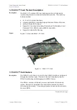
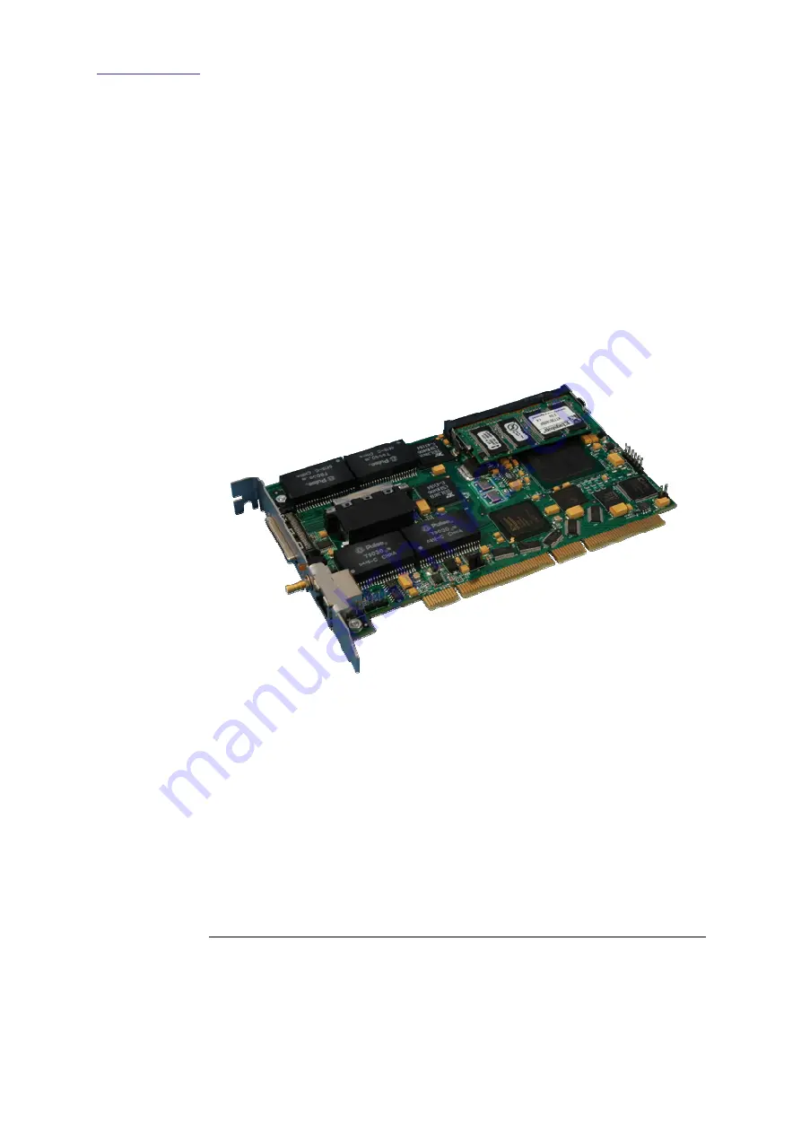
Figure 1-1 shows the DAG 3.7T Card. 


Figure 1-1.  DAG 3.7T Card. 


1.3 DAG 3.7T Architecture  

Description 

The TDM T1 or E1 data is received by the 16 RJ45 interfaces, and passed 
through line interface units.  The data is then fed immediately into the 
FPGA for deframing and demapping into HDLC frames.  
 
This FPGA contains an Ethernet processor and the DUCK timestamp 
engine.  Because of component close association, packets or cells are 
time-stamped accurately.  Time stamped packet records are then stored in 
the lower FIFO. 


Continued on next page 


Summary of Contents for DAG 3.7T

Page 1: ...EDM01 05 12r1 DAG 3 7T Card User Manual 2 5 5r1...

Page 2: ...19246 Hamilton 2001 New Zealand Phone 64 7 839 0540 Fax 64 7 839 0543 support endace com www endace com Endace USA Ltd Suite 220 11495 Sunset Hill Road Reston Virginia 20190 United States of America...

Page 3: ...These limits are designed to provide reasonable protection against harmful interference when the equipment is operated in a commercial environment This equipment generates uses and can radiate radio f...

Page 4: ...Options Supported 12 3 6 Inspect Interface Statistics 15 3 7 Configuring HDLC Channels 16 3 7 1 Configuring DAG 3 7T Card for Receive and Transmit 17 3 7 2 Timeslot Connection c 17 3 7 3 Delete Conne...

Page 5: ...ion 31 5 2 3 Card with Reference Time Synchronization 32 5 3 Synchronization Connector Pin outs 33 6 0 DATA FORMATS OVERVIEW 35 6 1 Data Formats 35 6 1 1 Generic Variable Length Record 35 6 1 2 Type 5...

Page 6: ...AG 3 7T Architecture DAG 3 7T Card Extended Functions DAG 3 7T Card System Requirements 1 1 User Manual Purpose Description The purpose of the DAG 3 7T Card User Manual is to identify and explain Inst...

Page 7: ...pport for receiving and sending Channelised Unchannelised and Fractional T1 E1 HDLC and non HDLC data traffic Support for data traffic filtering Figure Figure 1 1 shows the DAG 3 7T Card Figure 1 1 DA...

Page 8: ...Endace customer support team at support endace com to enable effective use of extended functions 1 5 DAG 3 7T Card System Requirements Description The DAG 3 7T card and associated data capture system...

Page 9: ...Endace Measurement Systems Limited http www endace com EDM01 05 12r1 DAG 3 7T Card User Manual Copyright all rights reserved 4 Version 6 22 September 2005 USE THIS SPACE FOR NOTES...

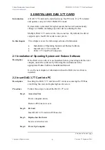
Page 10: ...m and Endace Software Insert DAG 3 7T Card into PC DAG 3 7T Card Port Connectors 2 1 Installation of Operating System and Endace Software Description If the DAG device driver is not installed before p...

Page 11: ...d there is also a VHDCI connector on the DAG 3 7T board itself The connector on the board allows a DAG 3 7T Pod to be used internally in a PC chassis in a spare 5 25 inch drive bay Use the connector o...

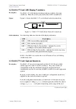
Page 12: ...er This chapter covers the following sections of information Interpreting DAG 3 7T Card LED Status DAG 3 7T Card LED Display Functions DAG 3 7T Card Capture Sessions Configuration in WYSYCC Style Conf...

Page 13: ...nization signal LED 4 PPS In Pulse Per Second In indicates the card is receiving an external clock synchronization signal NOTE The LED 4 is on when the Loss of Pointer or Loss of Framing conditions ar...

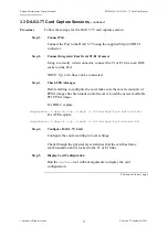
Page 14: ...NOTE Up to 16 lines can be connected Step 3 Check FPGA Images Before starting to configure the card make sure the most recent pair of FPGA images has been loaded onto the card Load the newest availabl...

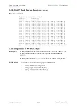
Page 15: ...link 8 mode 29 rxpkts txpkts nofcl eql term120 b8zs hdb3 E1 link 9 mode 29 rxpkts txpkts nofcl eql term120 b8zs hdb3 E1 link 10 mode 29 rxpkts txpkts nofcl eql term120 b8zs hdb3 E1 link 11 mode 29 rxp...

Page 16: ...b8zs hdb3 T1 ESF link 15 mode 29 rxpkts txpkts nofcl eql term120 b8zs hdb3 T1 ESF pci 33MHz 32 bit buf 32MB rxstreams 1 txstreams 1 mem 32 0 3 4 2 Configuring Card for Other Options Description For o...

Page 17: ...kts nofcl noeql term120 b8zs hdb3 T1 ESF link 12 mode 29 rxpkts txpkts nofcl noeql term120 b8zs hdb3 T1 ESF link 13 mode 29 rxpkts txpkts nofcl noeql term120 b8zs hdb3 T1 ESF link 14 mode 29 rxpkts tx...

Page 18: ...ittle to be concerned about with Transmit LBO Cabling There is two options in E1 75ohm unbalanced coaxial cable or 120ohm balanced twisted pair In T1 only standard is 100ohm balanced twisted pair Codi...

Page 19: ...T1 Short Haul 15dB 533 655 ft 3 0dB 100 TP B8ZS 13 T1 Short Haul 15dB Arbitrary Pulse 100 TP B8ZS 14 T1 Gain Mode 29dB 0 133 ft 0 6dB 100 TP B8ZS 15 T1 Gain Mode 29dB 133 266 ft 1 2dB 100 TP B8ZS 16 T...

Page 20: ...1 1 0 0 0 1 7 0 0 0 0 0 0 1 1 1 1 0 0 0 1 8 0 0 0 0 0 0 1 1 1 1 0 0 0 1 9 0 0 0 0 0 0 1 1 1 1 0 0 0 1 10 0 0 0 0 0 0 1 1 1 1 0 0 0 1 11 0 0 0 0 0 0 1 1 1 1 0 0 0 1 12 0 0 0 0 0 0 1 1 1 1 0 0 0 1 13 0...

Page 21: ...tool can be used to configure the DAG 3 7T card if it is running HDLC firmware Configuration file The configuration file is used to Configure HDLC channel connections Enable disable RAW Rx Each line...

Page 22: ...to configure a connection on interface 5 timeslot 16 it would look like c 0 5 16 0 5 16 3 7 3 Delete Connection d Description In order to delete a connection the connection must already exist This is...

Page 23: ...d is in RAW mode RAW mode is when no de framing or un bitstuffing is done Just the straight data from the timeslots read by the firmware This line would look like r ifc_num In order to configure a RAW...

Page 24: ...2 13 14 15 17 18 19 20 21 22 23 24 25 26 27 28 29 30 32 h 0 12 1 2 3 4 5 6 7 8 9 10 11 12 13 14 15 17 18 19 20 21 22 23 24 25 26 27 28 29 30 32 h 0 13 1 2 3 4 5 6 7 8 9 10 11 12 13 14 15 17 18 19 20 2...

Page 25: ...DLC firmware is a connection which occupies only one timeslot on one interface The line would look like c bit_offset ifc_num ts_num Captures using this configuration produce records with erf type 8 Th...

Page 26: ...7T card It reads a channel configuration file and then creates each of the channels defined in the file The default operation of dagchan is to delete all existing channel definitions on the board and...

Page 27: ...card has the appropriate transmit firmware image loaded 3 9 2 Timeslot Connection c Description A simple connection is a connection which occupies only one timeslot on one interface The line would loo...

Page 28: ...l Description A line connection is a connection which occupies all timeslots for example full line rate on 1 interface but is not in RAW mode This line would look like this l bit_offset ifc_num The bi...

Page 29: ...8 9 10 11 12 13 14 15 17 18 19 20 21 22 23 24 25 26 27 28 29 30 32 h 0 9 1 2 3 4 5 6 7 8 9 10 11 12 13 14 15 17 18 19 20 21 22 23 24 25 26 27 28 29 30 32 h 0 10 1 2 3 4 5 6 7 8 9 10 11 12 13 14 15 17...

Page 30: ...serial number 2 Host PC type and configuration 3 Host PC operating system version 4 DAG software version package in use 5 Any compiler errors or warnings when building DAG driver or tools 6 For Linux...

Page 31: ...e to each DAG card For example for HDLC capture with one DAG 3 7T card installed drv dagload tools dagrom rvp d dag0 f xilinx dag37tpci hdlc erf bit The integrity of the card s physical layer is then...

Page 32: ...ackets from the network link it writes a record for each packet into a large buffer in the host PC s main memory Avoiding packet loss In order to avoid packet loss the user application reading the rec...

Page 33: ...m Capture at OC 12 STM 4 622Mbps rates and above may require a larger buffer 128MB or more is suggested for Linux FreeBSD For the DAG 3 7T card Windows operating system the upper limit is 32MB In Debi...

Page 34: ...ed to avoid time variance between sets of DAG cards or between DAG cards and coordinated universal time UTC Accurate time reference can be obtained from an external clock by connecting to the DAG card...

Page 35: ...ternal input synchronize to host clock auxin Aux input unused rs422out Output the rs422 input signal loop Output the selected input hostout Output from host unused overout Internal output master card...

Page 36: ...e dagclock command must be rerun afterwards to restore the configuration 5 2 2 Two Cards no Reference Time Synchronization Description When two DAG cards are used in a single host PC with no reference...

Page 37: ...me receiver Pulse signal from external sources The DAG synchronization connector accepts a RS 422 Pulse Per Second PPS signal from external sources This is derived directly from a reference source or...

Page 38: ...agpps d dag0 The tool measures input state many times over several seconds displaying polarity and length of input pulse Some DAG cards have LED indicators for synchronization PPS signals 5 3 Synchron...

Page 39: ...and 6 The DAG card can also output a synchronization pulse used when synchronizing two DAG cards without a GPS input Synchronization output is generated on the Out A channel pins 1 and 2 Ethernet cro...

Page 40: ...In this section This section covers the following topics of information Generic Variable Length Record Type 5 Multi channel HDLC Frame Record Type 6 Multi channel RAW Link Data Record Type 7 Multi ch...

Page 41: ...e 6 TYPE_MC_RAW Multi channel Raw link data 7 TYPE_MC_ATM Multi channel ATM Cell flags This byte is divided into 2 parts the interface identifier and the capture offset 1 0 capture interface 0 3 2 var...

Page 42: ...3 BYTE 2 BYTE 1 BYTE 0 timestamp timestamp type 5 flags rlen lctr wlen MC Header HDLC header rlen 24 bytes of packet Table 6 2 Type 5 Multi channel HDLC Frame Record MC Header attributes The Type 5 M...

Page 43: ...set Table Table 6 3 shows the Type 6 Multi channel RAW Link Data record BYTE 3 BYTE 2 BYTE 1 BYTE 0 timestamp timestamp type 6 flags Rlen Lctr Wlen MC Header rlen 20 bytes of raw link data Table 6 3...

Page 44: ...BYTE 2 BYTE 1 BYTE 0 timestamp timestamp type 7 flags rlen lctr wlen MC Header ATM Header 48 bytes of cell Table 6 4 Type 7 Multi Channel ATM Cell Record MC Header attributes The Type 7 Multi channel...

Page 45: ...rted RX error is set if any MC header Error bit is set Table Table 6 5 shows the Type 8 Multi channel RAW Link Data record BYTE 3 BYTE 2 BYTE 1 BYTE 0 timestamp timestamp type 8 flags rlen lctr wlen M...

Page 46: ...ference between two timestamps can be found with a single 64 bit subtraction It is not necessary to check for overflows between the two halves of the structure as is needed when comparing Unix time st...

Reviews: