ENDEVCO 2680
INSTRUCTION MANUAL
IM2680
Page 4-3
G.
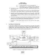
Non-linearity through this ran
ge should be less than 0.5% of
best straight line. Refer to
Product Data sheet, or paragraph 2.3.4 in Performance Specification for Amplitude
Linearity limits of Charge Amplifier under test.
4.
FREQUENCY RESPONSE
A.
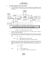
Connect equipment per Figure 4-1. Ensure J2 pin assignments conform to Charge
Amplifier being tested. See Note in Figure 4-1A.
B.
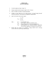
Energize equipment and allow 15 minutes to temperature stabilize.
C.
Adjust power supply or +28 V dc output.
D.
Adjust Oscillator Frequency for 100 Hz, and adjust Output Amplitude for 1.0 V rms output.
Oscillator output can be verified by setting test setting switch S1 to 1N position. The 1.0 V
rms must be checked prior to each reading of Charge Amplifier's Output in step 1.
E.
Remove positive (+) lead of DVM from test setup and connect lead to wiper of Voltage
Divider Potentiometer.
F.
Adjust Voltage Divider for a 1.0 V rms indication on DVM. This is an indication of Oscillator
Output in step D. This setting on Voltage Divider Potentiometer must be changed during
tests.
G.
Remove DVM positive (+) lead from wiper of Voltage Divider and reconnect as shown in
Figure 4-1 test setup.
H.
Set test setup switch S1 to 1N position. Verify Oscillator Output Amplitude is still 1.0 V rms
and then set switch to OUT position.
NOTE: A Charge Amplifier's frequency range of interest depends on type of filter used.
Refer to Table 1-3 for Model versus Frequency Range
I.
Vary Oscillator Frequency over Charge Amplifier's range of interest and observe
Oscilloscope and DVM for Gain versus Frequency Response. The Charge Amplifier's
Output Level must fall within limits listed in Table 1-3, or paragraph 2.3.2 in Performance
Specification.
5.
DC-TO-DC CONVERTER
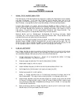
This test is performed only on Charge Amplifiers containing a DC-to-DC Converter (2681M1-M7).
The test checks the isolation between power ground and signal ground.
A.
Place a Shorting Cap on J1 INPUT Connector.
B.
Connect a magnetometer between Power-Ground Pin and Signal-Ground Pin on J2
OUTPUT Connector. Refer to Product Data Sheet on drawing in Performance Specification
for correct J2 pin assignment. As an example, J2 pin F is Power Ground and J2 pin D is
Signal Ground for 2681M1 through 2681M7.
C.
With magnetometer set to 50 V dc, the isolation between Power Ground and Signal Ground
shall be as specified in Product Data Sheet, or Power Supply isolation paragraph in
Performance Specification for Charge Amplifier under test. As an example, Charge
Amplifiers 2681M1-XXX through 2681M7-XXX shall have as isolation between both
grounds of 50
MΩ
or greater.


