background image


MicroGEA MX6 ULL HW manual 1.0.6

Getting started manual
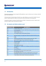
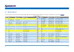
***** REV 1.0.6 *****

DATE

REVISION

CHANGE DESCRIPTION

29/11/2017

1.0.0

Release

21/02/2018

1.0.1

Proofread & correct grammar & added connector code for the Carrier board's interface

05/04/2018

1.0.2

Added connector information, moved chapter 7 to the adapter application notes

17/07/2018

1.0.3

Added Resistive Touch information. 

Updated sleep mode current consumption

18/07/2018

1.0.4

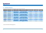
Updated ordering Information table

17/09/2018

1.0.5

Added in-rush current requirements during start-up

24/10/2018

1.0.6

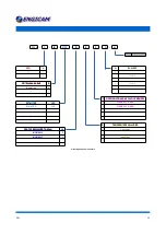
Updated ordering code, update mechanical information, updated LCD and touch connections chapter

D N :  

1

Summary of Contents for 0026700082I010

Page 1: ...05 04 2018 1 0 2 Added connector information moved chapter 7 to the adapter application notes 17 07 2018 1 0 3 Added Resistive Touch information Updated sleep mode current consumption 18 07 2018 1 0...

Page 2: ...serial port 24 5 5 How to connect CAN BUS interfaces 25 5 6 How to design the Ethernet interface 26 5 6 1 Component Placement considerations 28 5 6 2 Cable Transient Event and PHY Protection 29 5 6 3...

Page 3: ...1 Introduction This Chapter gives background information on this document Section includes General Overview Acronyms and Abbreviations Used Document and Standard References DN 3 Chapter 1 1...

Page 4: ...erter EMI Electromagnetic Interference high frequency disturbances ESD Electrostatic Discharge high voltage spike or spark that can damage electrostatic sensitive devices GND Ground GPIO General Purpo...

Page 5: ...Version 2 1 January 2000 Philips Semiconductor now NXP www nxp com I2S Bus Specification Feb 1986 and Revised June 5 1996 Philips Semiconductor now NXP www nxp com USB Specifications www usb org 1 3 2...

Page 6: ...2 Mechanical data This Chapter gives information about PCB and module s dimensions Section includes Mechanical data Assembly Top view Assembly Bottom view Interface Connectors DN 6 Chapter 2 2...

Page 7: ...wn top view assembly plan Figure 1 2 3 Assembly Bottom View The Figure below shows the bottom view assembly plan Figure 2 Note the connectors interface on module are HRS code DF40C 90DP that mates wit...

Page 8: ...llowing information report the connectors referred to the series DF40 HRS compliant with the MicroGEA SOM interface CARRIER CONNECTORS Note for information on the connectors positioning on carrier boa...

Page 9: ...on and Features This Chapter gives the ordering information and technical specifications of the modules Section includes MicroGEAMX6ULL Ordering code CPU memory specifications Operating temperature ra...

Page 10: ...D Single Ethernet Industrial i MX6ULL Industrial Temperature MCIMX6Y2 800MHz 512MB NAND 16 bit Memory temperature range industrial 40 to 105 40 to 85 4th Q 2026 MicroGEA MX6ULL 256MB LCD 0026700082I12...

Page 11: ...E B B 3 512MB No option 0 F F SPECIFICATIONNON VOLATILE MEMORY SPECIFICATIONNON VOLATILE MEMORY SOM TYPE SOM TYPE CCC CCC 0 256MB SLC NAND MicroGEA 008 1 512MB SLC NAND E E TEMPERATURE QUALIFIER TEMPE...

Page 12: ...4 Pinout This Chapter gives the pinout information Section includes Pinout overview i MX Pad spacifications Electrical specification DN 12 Chapter 4 4...

Page 13: ...BUS USB_OTG1_VBUS 5V power supply for USB OTG engine 13 NC Not Connect 14 USB_H1_VBUS USB_OTG2_VBUS 5V power supply for USB HOST engine 15 NC Not Connect 16 GND Ground 17 NC Not Connect 18 Vcoin CPU R...

Page 14: ...54 NC Not Connect 55 I2S_DOUT JTAG_TRST I2S Data Out 56 NC Not Connect 57 I2S_LRCLK JTAG_TDO I2S RCLK 58 NC Not Connect 59 I2S_SCLK JTAG_TDI I2S SCLK 60 NC Not Connect 61 GND Ground 62 NC Not Connect...

Page 15: ...ink led driver 14 DISP0_D9 1 LCD_DAT09 LCD parallel signal 15 3V3_ETH Power in 16 DISP0_D2 1 LCD_DAT02 LCD parallel signal 17 3V3_ETH Power in 18 DISP0_D3 1 LCD_DAT03 LCD parallel signal 19 3V3_ETH Po...

Page 16: ...NC Not Connect 57 GPIO2_IO12 ENET2_TX_DATA1 General GPIO 58 GND Ground 59 GPIO4_14 NAND_CE1 General GPIO 60 GND Ground 61 GPIO3_4 LCD_RESET General GPIO 62 I2C1_SCL CSI_PIXCLK I2C signal pull up neede...

Page 17: ...I_HSYNC uSDHC2 cmd signal 88 SD1_CMD SD1_CMD uSDHC1 cmd signal 89 GND Ground 90 GND Ground Table 3 The yellow rows highlight the required minimum electrical connections in order to make the module wor...

Page 18: ...3 GPIO V il 0 1 Table 4 1 This measure has done testing the module s start at the limit temperatures of 40 C and 85 C Module Test condition Current Vin Min Current Vin Typ Current Vin Max MicroGEA Lin...

Page 19: ...chnical specifications for carrier board design Section includes Carrier Board recommendations Power signals and backup battery Serials CAN Bus Ethernet USB SDIO LCD EPD Resistive Touch screen Boot mo...

Page 20: ...prove the planarity of ended board and optimize the process maintaining the electrical characteristics unchanged 5 1 3 Power Supply It s strongly recommended that the power supply of the carrier board...

Page 21: ...e shown the module power supply pins numbering Connect all power supply pins in order to avoid damage A connector B connector Name Primary Function Description GPIO Capable Voltage 19 3 3V Power PIN N...

Page 22: ...backup battery The connection with module is obtained by connecting directly the backup battery to the Vcoin signal pin 18 floating if not used Note The module is already designed to manage the charg...

Page 23: ...on the module s UART pins are 3 3V logic level this cannot be connected directly to a RS232 device like a PC Serial port the use of a transceivers on the base board is mandatory in order to avoid modu...

Page 24: ...also UART 4 5 can be used to connect a RS485 transceiver Figure 5 The pins involved in this RS485 communication example are listed in the following table A Connector Name Primary Function Description...

Page 25: ...CAN buses have been implemented Figure 6 The following table describes the pins numbering in the main connector involved in the CAN interface A Connector Name Primary Function Description CPU Pin Name...

Page 26: ...net interface to module Figure 7 The table below lists all Ethernet signal of the module B Connector Name Primary Function Description CPU Pin Name GPIO Capable Voltage 27 ETH_TXN Fast Ethernet TXN si...

Page 27: ...e g R1 in the figure to allow the directly connection of 3V3_ETH with 3V3 To optimize the SOM current consumption during power down state Engicam has arranged the power supply of the PHY Ethernet to...

Page 28: ...e edge of PCB up to the magnetics If the magnetics are integrated into RJ45 the differential pair should be routed to the back of integrated magnetics RJ45 connector away from the board of PCB 5 The 4...

Page 29: ...n any DC component other than the typical 3 3V pull up on the center tap of the transformer for analog signal biasing Especially in POE applications there are two main reasons why cable transient even...

Page 30: ...cross the TX pair in the figure below the voltage is clamped at a value equivalent to the forward bias voltage across D1 plus the zener voltage of D2 This transient voltage must be clamped at a voltag...

Page 31: ...wing table are listed all USB OTG signal of mail connector Use of the USB OTG port as Device or as Host depending on the status of the ID signal that is used also to enable the power supply Figure 12...

Page 32: ...s to connect the USB OTG interface that may be used to work as either a host or a device Use of the USB OTG port as a Host with its own dedicated supply The ID signal is forced to GND Figure 13 Use of...

Page 33: ...the Module Figure 15 A Connector Name Primary Function Description CPU Pin Name GPIO Capable Voltage 14 USB_VBUS USB HOST interface USB_OTG2_VBUS N 10 USB_DP USB HOST interface USB_OTG2_DP N 8 USB_DN...

Page 34: ...ule in the evaluation board The uSDHC signal of the module s main connector are listed in the table below Figure 16 B Connector Name Primary Function Description CPU Pin Name GPIO Capable Voltage 73 S...

Page 35: ...ISP0_D6 LCD interface LCD_DAT06 GREEN 0 Y 3 3V 36 DISP0_D7 LCD interface LCD_DAT07 GREEN 1 Y 3 3V 20 DISP0_D8 LCD interface LCD_DAT08 GREEN 2 Y 3 3V 14 DISP0_D9 LCD interface LCD_DAT09 GREEN 3 Y 3 3V...

Page 36: ...ce LCD_DAT09 GREEN 1 Y 3 3V 2 DISP0_D10 LCD interface LCD_DAT10 GREEN 2 Y 3 3V 6 DISP0_D11 LCD interface LCD_DAT11 GREEN 3 Y 3 3V 8 DISP0_D12 LCD interface LCD_DAT12 GREEN 4 Y 3 3V 10 DISP0_D13 LCD in...

Page 37: ...CLK Source driver shift clk LCD_CLK 3 3V 49 EPDC_VCOM00 Panel VCOM LCD_DAT19 3 3V 61 EPDC_GDOE gate driver output enable LCD_RESET 3 3V 10 EPDC_BDR00 Panel border control sw controlled LCD_DAT13 3 3V...

Page 38: ...DC hardware trigger function and control switches in touch screen analogue block Figure 17 A Connector Name TSC Function Description CPU Pin Name GPIO Capable Voltage 3 OSC_32KHZ_OUT Touch Screen_XR G...

Page 39: ...he following table lists the possible options of the boot mode BOOT_MODE1 PIN 49 BOOT_MODE0 PIN 47 Action 0 0 Boot From Fuses 0 1 Serial Downloader 1 0 Internal Boot DEFAULT 1 1 Reserved Table 19 BOOT...

Page 40: ...closing the jumper the module start from SD card Figure 18 Following you can see the signals logical level to implement a custom starting sequence The first sequence is already implemented in the mod...

Page 41: ..._CFG2 6 4 DISP0_D15 Floating BOOT_CFG2 7 51 GPIO3_28 Floating BOOT_CFG4 0 47 GPIO3_27 Floating BOOT_CFG4 1 3 UART8_RXD Floating BOOT_CFG4 2 1 UART8_TXD Floating BOOT_CFG4 3 49 GPIO3_24 Floating BOOT_C...

Page 42: ...Figure 19 Following the I2S BUS pins mapping A Connector Name Primary Function Description Pin Name on i MX GPIO Capable Voltage 53 I2S_DIN I2S Data In JTAG_TCK Y 3 3V 55 I2S_DOUT I2S_Data OUT JTAG_TR...

Page 43: ...6 Peripheral multiplexing This Chapter gives the alternative peripheral information Section includes I2S SPI PWM I2C UART CSI SD CAN DN 43 Chapter 6 6...

Page 44: ...3 3V 74 1 LCD_DAT20 SCLK 3 3V 68 CSI_DATA04 3 LCD_DAT21 SS0 3 3V 70 CSI_DATA05 30 LCD_DAT05 SS1 3 3V 28 LCD_DAT06 SS2 3 3V 36 LCD_DAT07 SS3 3 3V Table 23 ECSPI2 signals interfaces Pin on connector A P...

Page 45: ...I2S_LRCLK 3 3V 68 CSI_DATA04 Table 26 IIS2 bus interfaces Pin on connector A Pin on connector B Pin Name on i MX MicroGEA Signal reference Voltage reference 53 JTAG_TCK I2S_DIN 3 3V 55 JTAG_TRST I2S_D...

Page 46: ...croGEA Signal reference Voltage reference 35 26 GPIO_IO08 LCD_DAT00 PWM 1 3 3V 25 24 GPIO_IO09 LCD_DAT01 PWM 2 3 3V 27 16 GPIO_IO04 LCD_DAT02 PWM 3 3 3V 33 18 GPIO_IO05 LCD_DAT03 PWM 4 3 3V 39 LCD_DAT...

Page 47: ...SYNC I2C2_SCL 3 3V 75 UART5_TX_DATA 48 85 GPIO1_IO01 CSI_VSYNC I2C2_SDA 3 3V 73 UART5_RX_DATA Table 31 IIC3 Interfaces Pin on connector A Pin on connector B Pin Name on i MX MicroGEA Signal reference...

Page 48: ..._TX_DATA UART2_CTS Output 3 3V 71 UART2_CTS_B 36 UART3_RX_DATA UART2_RTS Input 3 3V 69 UART2_RTS_B 67 UART2_TX_DATA UART2_TXD Output 3 3V 65 UART2_RX_DATA UART2_RXD Input 3 3V Table 35 UART3 interface...

Page 49: ...TA0 UART6_TXD Output 3 3V 64 CSI_MCLK 37 ENET2_RX_DATA1 UART6_RXD Input 3 3V 62 CSI_PIXCLK Table 39 UART7 interfaces Pin on connector A Pin on connector B Pin Name on i MX MicroGEA Signal reference Vo...

Page 50: ...D3 3 3V 86 SD1_CLK SD1_CLK 3 3V 88 SD1_CMD SD1_CMD 3 3V Table 42 SD2 Pin on connector A Pin on connector B Pin Name on i MX MicroGEA Signal reference Voltage reference 9 GPIO1_IO07 SD2_CD 3 3V 64 CSI_...

Page 51: ...erence 88 20 UART3_CTS_B LCD_DAT08 CAN1_TX 3 3V 84 SD1_DATA0 90 14 UART3_RTS_B LCD_DAT09 CAN1_RX 3 3V Table 44 CAN 2 BUS Interface Pin on connector A Pin on connector B Pin Name on i MX MicroGEA Signa...

Page 52: ...oftware implementers to use Engicam products Engicam does not guarantee that the information in this manual is up to date correct complete or of good quality Nor does Engicam assume guarantee for furt...

Reviews: