background image

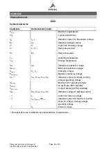
Symbols and terms

CeraDiode

Semiconductor diode

C

max

Maximum capacitance

C

typ

Typical capacitance

I

BR

I

R

, I

T

(Reverse) current @ breakdown voltage

I

leak

I

RM

(Reverse) leakage current

I

PP

I

PP

Current @ clamping voltage

I

PP

I

P

, I

PP

Peak pulse current

P

PP

P

PP

Peak pulse power

T

op

Operating temperature

T

stg

Storage temperature

V

BR

V

BR

(Reverse) breakdown voltage

V

BR,min

Minimum breakdown voltage

V

clamp

V

cl,

V

C

Clamping voltage

V

clamp,max

Maximum clamping voltage

V

DC

V

RM

, V

RWM

, V

WM

, V

DC

(Reverse) stand-off voltage, working
voltage, operating voltage

V

DC,max

Maximum DC operating voltage

V

ESD,air

Air discharge ESD capability

V

ESD,contact

Contact discharge ESD capability

V

leak

V

RM

, V

RWM

, V

WM

, V

DC

(Reverse) voltage @ leakage current

- *)

I

F

Current @ forward voltage

- *)

I

RM

, I

RM,max

@V

RM

(Reverse) current @ maximum reverse
stand-off voltage, working voltage,
operating voltage

- *)

V

F

Forward voltage

*) Not applicable due to bidirectional characteristics of CeraDiodes

CeraDiodes

High-speed series

Page 18 of 22

Please read Cautions and warnings and
Important notes at the end of this document.

Summary of Contents for CDA3C05GTH

Page 1: ...ed series Series Type Date August 2012 EPCOS AG 2012 Reproduction publication and dissemination of this publication enclosures hereto and the information contained therein without EPCOS prior express consent is prohibited ...

Page 2: ...era etc EDP products desktop and notebook computer monitor PDA printer memory card control unit head set speaker HDD optical drive etc Industrial applications Mobile phone applications Design Multilayer technology Nickel barrier termination Ag Ni Sn for lead free soldering Marking Due to the symmetrical configuration no marking information is needed Single chip 4 fold array 2 4 data 1 supply Gener...

Page 3: ...uctor diode equivalent CDS1C05GTH1 B72440C0050H160 5 5 17 33 7 CDS1C05GTH2 B72440C0050H260 5 5 20 66 3 CDS1C05GTH B72440D0050H060 5 6 21 70 6 10 Single 0402 SOD 723 CDS2C05HDMI1 B72590D0050H160 5 6 150 0 6 0 9 CDS2C05HDMI2 B72590D0050H260 5 6 90 0 6 0 9 CDS2C12GTH B72590D0120H060 12 20 66 4 5 CDS2C15GTH B72590D0150H060 15 23 66 10 15 CDS2C16GTH B72590D0160H060 16 65 290 2 3 CDS2C20GTH B72590D0200H...

Page 4: ... 4 0 13 0 75 Array devices 4 fold array 2 4 data 1 supply Dimension in mm Case size inch mm 0506 1216 0508 1220 0612 1632 1012 2532 Min Max Min Max Min Max Min Max l 1 50 1 70 1 8 2 2 3 0 3 4 2 90 3 50 w 1 20 1 40 1 05 1 45 1 45 1 75 2 25 2 75 h 0 6 0 9 0 9 1 2 d 0 2 0 4 0 2 0 4 0 25 0 55 0 35 0 65 e 0 4 0 6 0 4 0 6 0 61 0 91 0 8 1 1 k 0 35 0 35 0 35 0 45 CeraDiodes High speed series Page 4 of 22 ...

Page 5: ... 0 8 C 0 3 0 5 1 0 1 45 Array devices 4 fold array 2 4 data 1 supply Dimensions in mm Case size inch mm 0506 1216 0508 1220 0612 1632 1012 2532 A 0 36 0 35 0 5 0 7 B 0 84 0 9 0 7 1 0 C 0 62 0 4 1 2 1 4 E 0 50 0 5 0 76 0 95 CeraDiodes High speed series Page 5 of 22 Please read Cautions and warnings and Important notes at the end of this document ...

Page 6: ... P1 GND P2 GND P3 GND P4 GND P5 I O line 1 P6 I O line 2 P7 I O line 3 P8 I O line 4 2 4 data 1 supply Pin Description P1 I O line 1 P2 GND P3 I O line 2 P4 I O line 3 P5 VDC P6 I O line 4 CeraDiodes High speed series Page 6 of 22 Please read Cautions and warnings and Important notes at the end of this document ...

Page 7: ...Termination Single device Array device CeraDiodes High speed series Page 7 of 22 Please read Cautions and warnings and Important notes at the end of this document ...

Page 8: ...90D0150H060 0402 Cardboard 180 10000 CDS2C16GTH B72590D0160H060 0402 Cardboard 180 10000 CDS2C20GTH B72590D0200H060 0506 Blister 180 3000 CDA3C05GTH B72755D0050H062 0508 Cardboard 180 4000 CDA4C16GTH B72714D0160H060 0603 Cardboard 180 4000 CDS3C05HDMI1 B72500D0050H160 0603 Cardboard 180 4000 CDS3C16GTH B72500D0160H060 0603 Cardboard 180 4000 CDS3C30GTH B72500D0300H060 0612 Blister 180 3000 CDA5C16...

Page 9: ...le to center compartment P2 2 0 0 05 2 0 2 0 2 0 2 0 0 05 Pitch of component compartments P1 2 0 0 05 2 0 4 0 4 0 4 0 0 1 Tape width W 8 0 0 3 8 0 8 0 8 0 8 0 0 3 Distance edge to center of hole E 1 75 0 1 1 75 1 75 1 75 1 75 0 1 Distance center hole to center compartment F 3 5 0 05 3 5 3 5 3 5 3 5 0 05 Distance compartment to edge G 1 35 min 0 75 0 75 0 75 0 75 min Thickness tape T 0 35 0 02 0 6 ...

Page 10: ... 0 4 0 0 11 Distance center hole to center compartment P2 2 0 2 0 2 0 0 05 Pitch of component compartments P1 4 0 4 0 4 0 0 1 Tape width W 8 0 8 0 8 0 0 3 Distance edge to center of hole E 1 75 1 75 1 75 0 1 Distance center hole to center compartment F 3 5 3 5 3 5 0 05 Distance compartment to edge G 0 75 0 75 0 75 min Thickness tape T 0 3 0 3 0 3 max Overall thickness T2 1 3 2 5 2 5 max 1 0 2 mm o...

Page 11: ...cking units Case size inch mm 180 mm reel pieces 330 mm reel pieces Tape 0201 0603 15000 cardboard 0402 1005 10000 50000 cardboard 0603 1608 4000 16000 cardboard 1003 2508 4000 16000 cardboard 0506 1216 3000 12000 blister 0508 1220 4000 16000 cardboard 0612 1632 3000 12000 blister 1012 2532 2000 8000 blister CeraDiodes High speed series Page 11 of 22 Please read Cautions and warnings and Important...

Page 12: ...0 C2 Time tP 3 within 5 C of specified classification temperature Tc 20 s3 30 s3 Average ramp down rate Tp to Tsmax 6 C s max 6 C s max Time 25 C to peak temperature maximum 6 min maximum 8 min 1 Tolerance for peak profile temperature TP is defined as a supplier minimum and a user maximum 2 Depending on package thickness For details please refer to JEDEC J STD 020D 3 Tolerance for time at peak pro...

Page 13: ...components on the board It is best to mount the components on the board before soldering so that one termination does not enter the oven first and the second termination is soldered subsequently The ideal case is simul taneous wetting of both terminations 3 3 Solder joint profiles If the meniscus height is too low that means the solder quantity is too low the solder joint may break i e the compone...

Page 14: ...ickel barrier termination Good and poor solder joints caused by amount of solder in infrared reflow soldering CeraDiodes High speed series Page 14 of 22 Please read Cautions and warnings and Important notes at the end of this document ...

Page 15: ... activated flux without preheating at 255 5 C for 10 1 s No leaching of contacts Tests of resistance to soldering heat for SMDs IEC 60068 2 58 Immersion in 60 40 SnPb for 10 s at 260 C Immersion in Sn96 5Ag3 0Cu0 5 for 10 s at 260 C Capacitance change 15 C 15 Note Leaching of the termination Effective area at the termination might be lost if the soldering temperature and or immersion time are not ...

Page 16: ...applied smoothly to the end surface to a height of min 0 2 mm 5 5 Selection of flux Used flux should have less than or equal to 0 1 wt of halogenated content since flux residue after soldering could lead to corrosion of the termination and or increased leakage current on the surface of the CeraDiode Strong acidic flux must not be used The amount of flux applied should be carefully controlled since...

Page 17: ...n excessively long soldering time or high soldering temperature results in leaching of the out er electrodes causing poor adhesion due to loss of contact between electrodes and termina tion Avoid manual soldering with a soldering iron Wave soldering must not be applied for CeraDiodes designated for reflow soldering only Keep to the recommended down cooling rate 5 9 Standards CECC 00802 IEC 60068 2...

Page 18: ...max Maximum clamping voltage VDC VRM VRWM VWM VDC Reverse stand off voltage working voltage operating voltage VDC max Maximum DC operating voltage VESD air Air discharge ESD capability VESD contact Contact discharge ESD capability Vleak VRM VRWM VWM VDC Reverse voltage leakage current IF Current forward voltage IRM IRM max VRM Reverse current maximum reverse stand off voltage working voltage opera...

Page 19: ...on if a CeraDiode has insufficient time to cool down between a number of pulses occurring within a specified isolated time period Ensure that elec trical characteristics do not degrade Consider derating at higher operating temperatures Choose the highest voltage class compati ble with derating at higher temperatures Surge currents beyond specified values will puncture a CeraDiode In extreme cases ...

Page 20: ...racks to develop on the product and its parts which might lead to reduced reliability or lifetime Mounting When CeraDiodes are encapsulated with sealing material or overmolded with plastic material be aware that potting sealing or adhesive compounds can produce chemical reactions in the CeraDiode ceramic that will degrade its electrical characteristics and reduce its lifetime Make sure an electrod...

Page 21: ...minals Avoid dewing and condensation EPCOS CeraDiodes are designed for encased applications Under all circumstances avoid ex posure to direct sunlight rain or condensation steam saline spray corrosive gases atmosphere with reduced oxygen content EPCOS CeraDiodes are not suitable for switching applications or voltage stabilization where static power dissipation is required CeraDiodes are designed f...

Page 22: ...nt 3 The warnings cautions and product specific notes must be observed 4 In order to satisfy certain technical requirements some of the products described in this publication may contain substances subject to restrictions in certain jurisdictions e g because they are classed as hazardous Useful information on this will be found in our Ma terial Data Sheets on the Internet www epcos com material Sh...

Reviews: