background image

REV.-A

DISASSEMBLY, ASSEMBLY, AND ADJUSTMENT

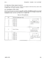
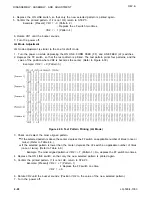
4.3.2 Bidirectional Printing Alignment Adjustment

This adjustment is required when the lines or characters are misaligned in bidirectional printing, and also when
the PBMA board or the printer mechanism is replaced.

4.3.2.1 Specifications of VR1 and VR2

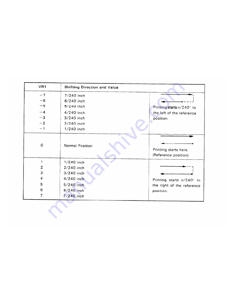
Bidirectional printing alignment is adjusted by 

using VR1 and VR2 on the PBMA board. VRl is used in draft

mode and VR2 is used in LQ mode. The specifications of VR1 and VR2 are shown 

in Tables 4-4 and 4-5. The

misalignment 

usually occurs when the carriage moves from 

right to left.

Table 4-4. VR1 Specifications

LQ-500/ L-1000

4-25

Summary of Contents for ActionPrinter L-1000

Page 1: ...LQ 500 L 1000 TECHNICAL MANUAL EPSON ...

Page 2: ...and receiver are on different branch circuits If necessary the user should consult the dealer or an experienced radio television technician for additional suggestions The user may find the following booklet prepared by the Federal Communications Commis sion helpful How to Identify and Resolve Radio TV Interference Problems This booklet is available from the U S Government Printing Office Washingto...

Page 3: ...REV A REVISION SHEET iv LQ 500 L 1000 ...

Page 4: ...ECT THE UNIT TO A POWER SOURCE UNTIL INSTRUCTED TO DO SO WHEN THE POWER SUPPLY CABLE MUST BE CONNECTED USE EXTREME CAUTION IN WORK ING ON POWER SUPPLY AND OTHER ELECTRONIC COMPONENTS WARNING 1 Repairs on Epson products should be performed only by an Epson certified repair technician 2 Make certain that the source voltage is the same as the rated voltage listed on the serial number rating plate If ...

Page 5: ... precautions on the preceding page The chapters are organized as follows Chapter 1 Provides a general product overview lists specifications and illustrates the main components of the printer Chapter 2 Describes the theory of printer operation Chapter 3 Discusses the options Chapter 4 Includes a step by step guide for product disassembly assembly and adjustment Chapter 5 Provides Epson approved tec...

Page 6: ...TENTS CHAPTER 1 CHAPTER 2 CHAPTER 3 CHAPTER 4 CHAPTER 5 CHAPTER 6 APPENDIX PRODUCT DESCRIPTION PRINCIPLES OF OPERATION OPTIONAL EQUIPMENT DISASSEMBLY ASSEMBLY AND ADJUSTMENT TROUBLESHOOTING MAINTENANCE LQ 500 L 1000 i x ...

Page 7: ...nting 1 19 1 6 4 Error Conditions 1 20 1 6 5 Buzzer Operation 1 20 1 6 6 Printer Initialization 1 20 1 6 7 Default Values 1 21 1 6 8 Adjust Lever Operation 1 21 1 6 9 Printer Protection for Heavy Duty Printing 1 22 1 7 MAIN COMPONENTS 1 23 1 7 1 PBMA Board 1 23 1 7 2 PEBPNL Board 1 24 1 7 3 PEBFIL Board 1 25 1 7 4 Transformer 1 26 1 7 5 Printer Mechanism M 5410 1 27 1 7 6 Housing 1 28 LIST OF FIGU...

Page 8: ...face Options 1 1 TABLE 1 2 Optional Units 1 1 TABLE 1 3 Cut Sheet Specifications 1 3 TABLE 1 4 Continuous Sprocket Paper Specifications 1 4 TABLE 1 5 Printing Mode 1 8 TABLE 1 6 Character Matrix and Character Size 1 9 TABLE 1 7 Connector Pin Assignments and Signal Functions 1 11 TABLE 1 8 Printer Select Deselect Control 1 13 TABLE 1 9 Settings for DIP Switch 1 SWI 1 14 TABLE 1 10 Settings for DIP ...

Page 9: ...in LQ fonts Roman and Sans Serif 6 Optional Font Module to provide a wide variety of fonts 7 Front panel switch selection of Draft Roman Sans Serif or slot Optional Font Module font 8 Automatic paper loading function 9 Easy handling of cut sheets with the optional cut sheet feeder CSF The LQ 500 L 1000 is equipped with the standard EPSON 8 bit parallel interface Various interface options enable us...

Page 10: ...REV A GENERAL DESCRIPTION Printer Cover A Printer Cover B Figure 1 l Exterior View of the LQ 500 L I000 LQ 500 L 1000 1 2 ...

Page 11: ...ration 24 wires 12 x 2 staggered diameter 0 2 mm Figure 1 2 Pin Configuration Feeding Method Line Spacing Paper Insertion Paper Feed Speed Friction feed tractor feed pull tractor 1 6 inch or programmable in units of 1 l80 inch From rear 100 ms line at 1 6 inch feed 2 2 inches per second continuous feed Paper Specifications See Tables 1 3 and 1 4 Table 1 3 Cut Sheet Specifications LQ 500 L 1000 1 3...

Page 12: ...er Specifications Printable Area The figure below illustrates the printable area for cut sheets 1 3 mm or more using 182 mm to 229 mm 7 2 in to 9 in width paper 27 mm or more using 257 mm 10 1 in width paper Figure 1 3 Cut Sheet Printable Area 1 4 LQ 500 L 1000 ...

Page 13: ...m 4 in to 9 5 in width paper 26 mm or more using 254 mm 10 in width paper l 2 13 mm or more using 101 mm to 242 mm 4 in to 9 5 in width paper 24 mm or more using 254 mm 10 in width paper Figure 1 4 Printable Area for Continuous Sprocket Feed Paper LQ 500 L 1000 1 5 ...

Page 14: ...ting Current Insulation Resistance Dielectric Strength 120 VAC 10 120 V version 220 VAC 10 220 V version 240 VAC 10 240 V version 49 5 to 50 5 Hz 50 Hz version 59 5 to 60 5 Hz 60 Hz version 1 8A 120 V version 0 9A 220 V version 0 9A 240 V version 10 Megohms min Between AC Line and Chassis Between AC Line and Chassis 1250 VAC rms 1 minute 120 V version 3750 VAC rms 1 minute 220 240 V version Enviro...

Page 15: ...will be ignored 8 bits 96 ASCII and 13 international character sets EPSON Roman Family number 0 EPSON Sans Serif Family number 1 EPSON Roman 10 EPSON Roman 12 EPSON Roman 15 EPSON Roman Proportional EPSON Sans Serif 10 EPSON Sans Serif 12 EPSON Sans Serif 15 EPSON Sans Serif Proportional EPSON Draft 10 EPSON Draft 12 EPSON Draft 15 Selection and mixture of the following modes are allowed except 15...

Page 16: ...S 1 Max means the value when characters of the maximum width were printed 2 Min means the value when characters of the minimum width were printed 3 means that LQ character set is automatically selected when proportional pitch is specified 1 8 LQ 500 L 1000 ...

Page 17: ...alue will be changed by differences in paper ribbon etc 3 Unit ESC sp which also can be sent as the unit followed by the character string CHR h20 indicates the minimum length to be added to the right of the character that can be specified with the ESC sp control code 4 4 indicates that character matrix is reshaped by printer firmware Character width becomes half of noncondensed character width LQ ...

Page 18: ...GENERAL DESCRIPTION REV A Figure 1 5 Character Matrix 1 10 LQ 500 L 1000 ...

Page 19: ... Signal Level Adaptable Connector Data Transmission Timing 8 bit parallel By STROBE pulse By BUSY and ACKNLG signal TTL compatible 57 30360 Amphenol or equivalent See Figure 1 6 Figure 1 6 Data Transmission Timing Table 1 7 shows the connector pin assignments and signal functions of the 8 bit parallel interface Table 1 7 Connector Pin Assignments and Signal Functions LQ 500 L 1000 1 11 ...

Page 20: ...nterface conditions are based on TTL levels Both the rise and fall times of all signals must be less than 0 2 µs 5 The AUTO FEED XT signal can be set at LOW by DIP switch 2 4 6 The SELECT IN signal can be set at LOW by jumper 6 7 Printing tests including those of the interface circuits can be performed without using external equipment by setting DATA 1 8 of the interface connector to certain codes...

Page 21: ...selected state unless the DC1 code is input again In the deselected state the printer ignores input data until the DC1 code is received 3 The DC1 and DC3 codes are enabled only when the SLCT IN signal Input Connector 36 for the parallel interface unit is HIGH and printer power is initialized 4 If the SLCT IN signal is LOW when the printer is initialized DC1 DC3 printer select deselect control is i...

Page 22: ...e located inside the ROM cartridge slot cover and function as shown in Tables 1 9 through 1 13 Note that the status of the DIP switches is read only at power on or upon receipt of the INIT signal Table 1 9 Settings for DIP Switch 1 SW1 Unidirectional printing is selected by default however input of ESC U O can be used to set the print direction to Bidirectional Table 1 11 International Character S...

Page 23: ...er is connected the SLCT IN signal is fixed to LOW and DC1 DC3 printer select control is ignored 1 5 SELECTYPE FUNCTION Selectype allows the user to choose fonts easily while the printer is ON LINE This function provides for selec tion of Draft Roman Sans Serif or the slot ROM cartridge font SelecType is effective only when the printer is ON LINE and is not printing Font selection is performed by ...

Page 24: ...INE FEED button To begin printing the self test using the Letter Quality LQ mode turn the printer power ON while pressing FORM FEED Self test printing can be stopped or started by pressing ON LINE ON LINE indicator is not lit To finish the self test stop the printing by pressing the ON LINE switch and turn OFF the printer power The firmware revision number is printed as the first line of the self ...

Page 25: ...UMP mode the hexadecimal representation of the input data is printed out along with corresponding ASCII characters This function is valuable for checking the data the printer has received from the host If input data is a control code rather than a character code a period is printed in the ASCII column D a t a D u m p M o d e Figure 1 8 Hexadecimal Dump Function LQ 500 L 1000 1 17 ...

Page 26: ...g half dots Double speed 240 dpi including half dots 1 5 speed 360 dpi including half dots Normal speed The firmware however implements the print densities as shown in Table 1 14 Table 1 14 Print Density NOTES ESC m n1 n2 DATA n2 x 256 n1 dpi dots per inch ips inches per second The firmware handles the print densities as shown in Table 1 15 Table 1 15 Bit Image Printing 1 18 LQ 500 L 1000 ...

Page 27: ...ond with a 0 1 second interval 0 When abnormal carriage movement is detected the buzzer sounds 5 times rings for 0 5 second with a 0 5 second interval l When a panel setting is accepted 0 1 second ring 1 6 6 Printer Initialization There are two initialization methods hardware initialization and software initialization Hardware Initialization This type of initialization takes place when the printer...

Page 28: ...per position becomes top of form position Released 116 inch Cleared Every 8 characters relative Channel 0 SelecType Software initialization DIP switch Hardware initialization Deselected Software initialization Cleared Hardware initialization Left justification 10 CPI ESC K ESC 0 ESC L ESC 1 ESC Y ESC 2 ESC Z ESC 3 Cleared 1 6 8 Adjust Lever Operation The head adjust lever must be set to the proper...

Page 29: ...ically stopped until head temperature has dropped to a certain value to resume printing If heavy duty printing causes the voltage supplied to the head drive circuit to drop to the lower limit then print ing is interrupted immediately and thereafter if power supply voltage is recovered to a certain value then the remaining print line will be printed This protection will occur when half or more of t...

Page 30: ... board 2 PEBPNL board 3 PEBFIL board 4 Transformer 5 M 5410 The main control board the CPU on this board controls all main functions The control panel board The filter circuit board The printer mechanism Figure 1 10 LQ 500 L 1000 Component Layout 1 7 1 PBMA Board The use of the µPD7810HG CPU makes the main control board simple in its circuit design Figure 1 11 PBMA Main Control Board 1 22 LQ 500 L...

Page 31: ...tor LEDs switches and buzzer Figure 1 12 PEBPNL Control Panel Board 1 7 3 PEBFIL Board The PEBFIL board eliminates noise from the AC line to the printer and from the printer to the outer line The fuse used on this board prevents overheating 120 V Version 220 240 V Version Figure 1 13 PEBFIL Filter Board LQ 500 L 1000 1 23 ...

Page 32: ...t board 120 V Version 220 V Version Figure 1 14 Transformer 240 V Version 1 7 5 Printer Mechanism M 5410 The M 5410 printer mechanism was developed expressly for use with LQ 500 L 1000 printer the components include a carriage motor carriage mechanism paper feed motor paper feed mechanism ribbon feed mechanism printhead and sensors Figure 1 15 Model 5410 Printer Mechanism 1 24 LQ 500 L 1000 ...

Page 33: ...f the upper and lower cases The upper case houses the control panel The lower case contains the printer mechanism and the main control board The printer cartridge is easily removable and can be replaced simply by lifting the upper case LQ 500 L 1000 Figure 1 16 Housing 1 25 ...

Page 34: ...lator Circuit 2 14 2 2 1 7 Pulse Width Modulation PWM Circuit 2 16 2 2 1 8 24 VDC Regulator Circuit 2 18 2 2 1 9 12 VDC Supply Circuit 2 20 2 2 1 10 Vx Voltage Supply Circuit 2 21 2 2 2 Reset Circuit 2 22 2 2 3 Firmware Operation at Reset 2 26 2 2 4 Address Decorder and Bank Register 2 30 2 2 5 Carriage Operation 2 32 2 2 5 1 Carriage Mechanism 2 32 2 2 5 2 Carriage Motor Specifications 2 32 2 2 5...

Page 35: ...GURES FIGURE 2 1 Cable Connectors 2 2 FIGURE 2 2 Printer Mechanism Block Diagram 2 3 FIGURE 2 3 Paper End Sensor 2 4 FIGURE 2 4 Home Position Sensor 2 4 FIGURE 2 5 Thermal Sensor Printhead Temperature Detection 2 5 FIGURE 2 6 Printhead 2 6 FIGURE 2 7 Circuit Block Diagram 2 7 FIGURE 2 8 Memory Map 64K Bytes 2 8 FIGURE 2 9 Power Supply Circuit Block Diagram 2 9 FIGURE 2 10 Step Down Circuit 2 11 FI...

Page 36: ...ess Module Removed 2 25 Initialization Program Flowchart 2 26 Memory Map 2 29 Carriage Mechanism 2 31 Carriage Drive Circuit Block Diagram 2 32 Gate Array Operation 2 33 Carriage Motor Drive Circuit 2 35 STK 6981 B Circuit Diagram 2 36 Reference Voltage Generation Circuit 2 37 Constant Current Control Circuit 2 38 Chopping Waveforms 2 39 Schmitt Trigger Circuit 2 40 Chopping Current and Drive Spee...

Page 37: ...BLE 2 21 LIST OF TABLES Board Connector Summary 2 1 Power Supply Applications 2 10 Control Commands 2 30 Control Commands 2 34 Reference Voltage 2 37 Current Values for Reference Voltages 2 39 Phase Excitation Method 2 41 Drive Sequence 2 2 Excitation 2 41 Drive Sequence 1 2 Excitation 2 42 Chopping Current 2 43 Time Constants for Speeds 2 43 Acceleration Time Data 2 2 Excitation 2 44 Deceleration...

Page 38: ...mechanism power supply circuits and control circuits The chapter also describes the operation of the printer s circuitry and printer mechanism 2 1 1 Summary of Connectors The interconnection of the primary components is shown in Figure 2 1 Table 2 l summarizes the function size and type of the connectors designated in the figure Table 2 1 Board Connector Summary LQ 500 L 1000 2 l ...

Page 39: ...PRINCIPLES OF OPERATION REV A 2 2 LQ 500 L 1000 Figure 2 1 Cable Connections ...

Page 40: ... Model 5410 printer mechanism is a serial impact dot matrix printer that prints at 180 dots per inch DPI in both the horizontal and vertical directions Figure 2 2 shows a block diagram of the Model 5410 printer mechanism Figure 2 2 Printer Mechanism Block Diagram LQ 500 L 1000 2 3 ...

Page 41: ... This sensor switch is ON when paper runs out Paper out state ON LOW level Paper present OFF HIGH level Figure 2 3 Paper End Sensor Home Position Sensor HP Sensor Figure 2 4 shows the home position sensor This sensor switch is ON when the carriage is at the home position Home position ON LOW level Other position OFF HIGH level The reference position for the carriage driver is determined by this se...

Page 42: ...rinthead temperature If head temperature exceeds the upper limit value then printing is automatically stopped until head temperature drops to a certain value before resum ing printing Figure 2 5 below illustrates the printer s thermal sensor circuit Figure 2 5 Thermal Sensor Printhead Temperature Detection LQ 500 L 1000 2 5 ...

Page 43: ...n and is controlled by an open loop system Paper Feed Motor Paper feeding is carried out by a 4 phase 48 step motor This unit is designed to advance the paper l 180 inch for each step phase switch using 2 2 phase excitation The motor is controlled by the CPU in an open loop configuration 2 1 2 3 Printhead Figure 2 6 shows the dot wire operation The head driving coil is energized so that the dot wi...

Page 44: ......

Page 45: ...2 1 4 Firmware Overview This printer has a µPD7810HG CPU with 64K bytes of address space Figure 2 8 shows a memory map of this address space NOTE CG character generator GA gate array Figure 2 8 Memory Map 64K Bytes 2 8 LQ 500 L 1000 ...

Page 46: ...input to the power supply circuit on the main board The 26 VAC are converted into about 36 VDC via the full wave rectifier and smoothing circuit and input to the regulator circuits for 24 VDC and 5 VDC to be supplied to the control circuit The 24 VDC and 5 VDC are also supplied to the Vx voltage circuit and while generating the Vx voltage transferred to the control circuit The 12 VAC supplies a no...

Page 47: ...PRINCIPLES OF OPERATION REV A Table 2 2 Power Supply Applications 2 10 LQ 500 L 1000 ...

Page 48: ...uit Figure 2 10 shows the chopper type step down switching regulator circuit When the transistor is ON voltage Vi is applied to coil L and capacitor C and load current IL flows At this time electromagnetic energy WL is accumulated in choke coil L When the transistor turns off energy WL is applied to the load via flywheel diode D so that output voltage Vo becomes the average value Figure 2 11 Step ...

Page 49: ...nter from going out via the AC line Either Cl or C2 drains leakage current between the primary coil and the case Figure 2 12 shows the filter circuit Figure 2 12 PEBFIL Filter Circuit Board 2 2 1 4 Transformer AC voltages 120 VAC 220 VAC 240 VAC that pass through the filter circuit are divided into 26 VAC and 12 VAC and supplied to the PBMA circuit Figure 2 13 shows a schematic drawing of the powe...

Page 50: ...e full wave rectified by diode bridge DB1 and con verted to approximately 36 VDC by smoothing capacitor C40 The 24 VDC and 5 VDC voltages are con verted from this DC voltage which is used as the power supply voltage for the switching regulator IC at the next stage Figure 2 14 Rectifier and Smoothing Circuit LQ 5001 L 1000 2 13 ...

Page 51: ...wn above employs an NJM2355 configured as a chopper style switching regulator circuit This IC has a built in oscillator The oscillation frequency is determined by external components connected to pins 2 and 3 Therefore R105 and C34 cause the circuit to oscillate at about 30 KHz The oscillator waveform is shown in Figure 2 16 Figure 2 15 5 V Regulator Circuit Figure 2 16 Oscillator Waveform 2 14 LQ...

Page 52: ...he positive and negative input terminals This has the effect of maintaining the voltage at the positive terminal at 5 V Figure 2 18 shows the output from AMP 1 When the voltage at pin 4 becomes higher than that at pin 5 over voltage AMP 1 outputs current modulated by pulse width modulation PWM to reduce the output voltage of the circuit PWM is described below Figure 2 17 Constant Voltage Control 5...

Page 53: ...the outputs from AMP 2 and AMP 3 in circuit 2 flow into the negative terminal of PWM comparator 2 without wired OR Dead time control voltage is also input to additional negative terminals of both PWM comparators 1 and 2 A sawtooth waveform from the oscillator is input to the positive terminals The sawtooth waveform from the oscillator causes the comparators to generate pulses as shown in Figure 2 ...

Page 54: ...JM2355 is lower than the preset voltage or current value it is controlled by the dead time control voltage When it exceeds the preset value it is controlled by the error amplifier to keep it lower than the preset value Figure 2 20 Output Transistor Drive Waveform LQ 5001 L 1000 2 17 ...

Page 55: ...C regulator circuit has almost the same function and employs the same oscillation circuit as the 5 VDC regulator circuit Here the error amplifier AMP 2 is used for over current control and AMP 3 for constant voltage control The operation of the error amplifier AMP Figure 2 21 24 V Regulator Circuit 2 18 LQ 500 L 1000 ...

Page 56: ... following value Figure 2 22 Constant Voltage Control 24 VDC AMP 2 operates as follows for over current control 24 V is applied to the negative terminal and the positive terminal will receive an equal voltage when based on Figure 2 23 a negative current of the following value flows Figure 2 23 Over Current Protection OCP Dead time control has no bearing in this case because pin 3 of IC1 is grounde...

Page 57: ...ed by diode D19 and is converted to 12 VDC As shown by Figure 2 24 the half wave rectified voltages pass through the capacitor smoothing circuit so that the ripple is small and the average DC voltage rises when no load current flows and drops as load current increases Figure 2 24 12 VDC Circuit 2 20 LQ 500 L 1000 ...

Page 58: ...revent abnormal operation of the printer when the power is switched on or off 0 Reset Circuit Power Supply When the power is switched on or off the circuit is reset so that it will not drive the printer until the power supply becomes stable 0 Pull ups for the Printhead Signal Lines These prevent printhead malfunctions when power is switched on or off 0 Pull ups for the Paper Feed Motor Signal Line...

Page 59: ... circuit when any of the following occurs 0 Power is turned on or off 0 The INIT signal is input from either the host interface or an optional interface l A module font or identity is mounted or removed Figure 2 26 Reset Circuit Power On or Off D14 R69 and C26 in Figure 2 26 comprise an ON OFF reset circuit The purpose of this circuit is to make the CPU start from address 0000 hex when power is ap...

Page 60: ...charging capacitor C26 via diode D14 The gate array pins 49 to 51 is used for waveform shaping Figure 2 27 RESET Output INIT Signal Input from CN1 or CN2 The external INIT signal 50 µsec or less is passed through the low pass filter of R31 and C22 and waveform shaped in the gate array pin 47 of IC6C to set the DISC terminal LOW discharge capacitor C26 and set the gate array THLD terminal LOW Follo...

Page 61: ... 6C and a LOW signal is correspondingly output from the DISC terminal and RESET is output from the ROUT terminal As the DISC terminal goes LOW capacitor C26 is discharged with a time constant R70 x C26 When the discharge of C26 reduces the potential at the THLD terminal to threshold voltage Vth the RESET signal is canceled and the DISC terminal goes HIGH After the DISC terminal goes HIGH Vx voltag...

Page 62: ...ay 6C receives a HIGH signal Then the DISC terminal outputs a LOW signal and the ROUT terminal outputs a RESET signal The remainder of the sequence is similar to that when a ROM cartridge is mounted so please refer to the preceding page Figure 2 29 RESET Pulse Oscillation Process Module Removed LQ 500 L 1000 2 25 ...

Page 63: ...et the CPU executes the initialization program from address 0000 hex When this program has completed normally the CPU enters the standby state and waits for data Figure 2 30 shows the initialization program flowchart Figure 2 30 Initialization Program Flowchart 2 26 LQ 500 L 1000 ...

Page 64: ...REV A PRINCIPLES OF OPERATION Figure 2 30 Initialization Program Flowchart Cont LQ 500 L 1000 2 2 7 ...

Page 65: ...PRINCIPLES OF OPERATION REV A Figure 2 30 Initialization Program Flowchart Cont 2 2 8 LQ 500I L 1000 ...

Page 66: ...C external CG RAM 2C HEAD gate array 7A via address lines AB12 through AB15 and bank lines 7 and 6 in the gate array However the chip select for the CS is generated in conjunction with the RD signal and that of the RAM is generated in conjunction with the ALE signal Software control of firmware can check whether an external PROM is mounted or not and if the correct PROM is mounted the memory map s...

Page 67: ...a bank register in gate array EOlA05KA 6C The bank lines are set by writing to address FO02 hex and they can be checked by reading the same address Table 2 3 shows the relationship between data bits and bank lines Table 2 3 Control Commands 2 30 LQ 500 L 1000 ...

Page 68: ...iage motor and moved via the belt driven pulley The printhead is mounted on the carriage and the entire unit is moved right and left along the carriage guide shaft and plate Figure 2 32 Carriage Mechanism 2 2 5 2 Carriage Motor Specifications Carriage motor specifications are as follows Type Drive Voltage Coil Resistance Current 4 phase 48 pole stepper motor 24 V f 10 21 ohms f 7 at 25 degrees C M...

Page 69: ...arriage motor drive circuit In this circuit the phase switching for the carriage motor is not directly executed by the CPU but by the gate array 6C using pulses from the CPU STK 6981 B is employed to drive the carriage motor using a stabilized current Figure 2 33 Carriage Drive Circuit Block Diagram 2 32 LQ 500 L 1000 ...

Page 70: ...rmed by gate array EOlA05KA 6C This gate array first sets the excitation system 2 2 phase or 1 2 phase and rotation direction clockwise Or counterclockwise Then after the CPU outputs a pulse to the TM terminal of the gate array executes auto phase switching to drive the stepper motor Figure 2 34 shows this process LQ 500 L 1000 Figure 2 34 Gate Array Operation 2 33 ...

Page 71: ... control port of the gate array is assigned to address FO03 hex Control commands for the carriage motor via the gate array are listed in Table 2 4 Table 2 4 Control Commands When power is turned on CW clockwise CCW counterclockwise 2 34 LQ 500 L 1000 ...

Page 72: ... motor with a constant current The value of the current is determined by an external voltage level The IC operation can be separated into phases AB and CD which are completely equivalent Phase CD is described here as a model Figure 2 35 shows the carriage motor drive circuit Figure 2 36 shows the STK 6981 B circuit diagram Figure 2 35 Carriage Motor Drive Circuit LQ 5001 L 1000 2 35 ...

Page 73: ...PRINCIPLES OF OPERATION REV A NOTE Phase AB is equivalent to the above Figure 2 36 STK 6981 B Circuit Diagram 2 36 LQ 500 L 1000 ...

Page 74: ...eference Voltage Generation Circuit Figure 2 37 shows the reference voltage generation circuit and Table 2 5 shows the reference voltage Figure 2 37 Reference Voltage Generation Circuit Table 2 5 Reference Voltage LQ 500 L 1000 2 37 ...

Page 75: ...B5 of the CPU is set HIGH the input to the chopping circuit becomes 0 V and current is applied from the 5 V line to the motor via resistor R1 and diode D1 This current is given by I 5 V VD15 VD5 R76 21 ohms phase R79 Figure 2 38 shows the constant current circuit Table 2 6 lists the current values for reference voltages 2 38 LQ 500 L 1000 Figure 2 38 Constant Current Control Circuit ...

Page 76: ...voltage a and the feedback voltage are compared by the comparator in IC1 If reference voltage a is HIGH TR6 turns on applying approximately 25 VDC to the coil The current rises linearly due to inductance and TR6 turns off when the feedback voltage reaches reference voltage In this manner an almost constant current can be applied to the coil Figure 2 39 shows the drive current waveform pin 12 of th...

Page 77: ...PRINCIPLES OF OPERATION 2 40 REV A Figure 2 40 Schmitt Trigger Circuit LQ 500 L 1000 ...

Page 78: ...trol Excitation System The excitation system is determined by the firmware and is executed in accordance with the carriage speed as shown in Table 2 7 The motor drive sequence for each excitation system is shown in Tables 2 8 and 2 9 Table 2 7 Phase Excitation Method Table 2 8 Drive Sequence 2 2 Excitation LQ 500 L 1000 2 41 ...

Page 79: ... motor control system is an open loop system which switches the phases in accordance with set speeds The drive chopping current is switched at the drive frequency for the carriage motor The relationship between drive speed and switching current value is shown in Figure 2 41 and values for the drive chopping current are listed in Table 2 10 Figure 2 41 Chopping Current and Drive Speed 2 42 LQ 500 L...

Page 80: ...celeration control and deceleration control are shown below The a marks in the acceleration and deceleration columns control items in the tables and indicate switching times from Al to A2 or 62 to B1 Figure 2 42 Carriage Motor Control Table 2 11 Time Constants for Speeds LQ 500 L 1000 2 43 ...

Page 81: ...PRINCIPLES OF OPERATION REV A Table 2 12 Acceleration Time Data 2 2 Excitation Table 2 13 Deceleration Time Data 2 2 Excitation 2 44 LQ 500 L 1000 ...

Page 82: ...REV A PRINCIPLES OF OPERATION Table 2 14 Acceleration Time Data 1 2 Excitation LQ 500 L 1000 2 45 ...

Page 83: ...PRINCIPLES OF OPERATION REV A Table 2 15 Deceleration Time Data 1 2 Excitation 2 46 LQ 500 L 1000 ...

Page 84: ... the home position seek operation After power is applied the printer executes 2 2 phase excitation for 20 or 30 ms and checks the HOME signal regardless of the phase switching timing The result of this check determines whether the starting position should be 1 or 2 The carriage enters the home position only once during the initialization Figure 2 43 Home Position Seek LQ 5001 L 1000 2 47 ...

Page 85: ...Printing Timing Abnormal Carriage Operation This unit does not employ a print timing signal PTS sensor and cannot detect abnormal carriage operation Therefore no error occurs even if carriage movement is prevented by external forces An error will only occur if the HOME signal is received in the printing area in which case the carriage will stop 2 48 LQ 500 L 1000 ...

Page 86: ...eed rollers and by the printer cover At this time the paper feed motor is driven to rotate the platen gear via the paper feed reduction gear in the direction shown in Figure 2 45 The rotation of the platen gear feeds the paper in the direction of the arrow due to friction from the paper feed rollers and platen Because the paper is held against the platen by the spring force of the paper feed rolle...

Page 87: ...o rotate the gears via the pinion on the shaft of the motor in the direc tion shown in Figure 2 46 Rotating the gears rotates the sprocket wheels which advances the paper in the direction shown by the arrow For the sprocket feed method the pressure of the paper feed rollers against the platen is released by shifting the release lever forward Figure 2 46 Sprocket Feed Operation 2 50 LQ 500 L 1000 ...

Page 88: ...0 30 A typical Holding 0 06 A f 20 mA 400 PPS 2 2 6 3 Paper Feed Motor Drive Circuit The paper feed motor drive circuit is shown in Figure 2 47 A stepper motor is used as the paper feed motor and the 2 2 phase excitation system is employed When the paper feed signal PB2 is set to LOW Q27 is turned on and 24 V is supplied to the motor When the paper feed motor is not being driven 5 V is supplied to...

Page 89: ... the 2 2 phase excitation system Table 2 16 shows the paper feed motor excitation system Table 2 16 Excitation Sequence Clockwise Paper Feeds Forward NOTE If the paper feed motor is driven counterclockwise paper is fed in reverse Figure 2 48 and Table 2 17 show the timing chart and the counter values for the acceleration and deceleration control respectively Figure 2 48 Paper Feed Motor Drive Timi...

Page 90: ...REV A PRINCIPLES OF OPERATION Table 2 17 Setting Time NOTE If steps are less than 10 the speed is neither accelerating nor decelerating LQ 500 L 1000 2 53 ...

Page 91: ... wire strikes the ribbon and the paper against the platen to print a dot in the paper When the head driving coil is deenergized the actuating plate returns to the initial position as a result of action of the actuating plate spring After striking the platen the dot wire also returns to its initial position as a result of impact energy and from the wire resetting spring and the dot wire is held in ...

Page 92: ... 16 f 10 at 25 degrees C 415 µs to 435 µs 1 111 msec 900 Hz f 5 0 12 A typical 2 2 7 3 Printhead Drive Circuit Block Diagram Gate array E05A02LA is used as an 8 bit x 3 data latch The CPU determines the pulse width for the head wire drive pulses from gate array E05A02LA by monitoring the printhead drive power 24 V line The CPU also monitors the printhead temperature and stops printing if it gets t...

Page 93: ...inthead data Figure 2 51 is a block diagram of the E05A02LA gate array The gate array mainly consists of data latches 8 bits x 3 24 bits The gate array has functions commands for writing data to all 24 bits of the data latches efficiently Figure 2 51 E05A02LA Block Diagram Because the CS terminal of this gate array is activated by accessing addresses F004 hex and FO05 hex the command output addres...

Page 94: ...ERATION Table 2 18 E05A02LA Gate Array Functions NOTE When HPW setting is invalid the HPW output will be in the open drain ON state independent of the HPW input The drive pulse is input to the HPW terminal LQ 500 L 1000 2 57 ...

Page 95: ...The drive pulse width is adjusted using CPU port PC6 The Vx voltage is used to pull up the output signals from the gate array in order to prevent printhead malfunctions Figure 2 52 Printhead Drive Circuit Figure 2 53 Printhead Driving Waveforms 2 58 LQ 500 L 1000 ...

Page 96: ...eet the specifica tions of the printhead solenoid drive frequency 900 Hz The drive pulse width is adjusted by using an A D converter to detect the drive voltage and is kept within the area shown by the oblique lines in Figure 2 55 Figure 2 54 Print Timing Figure 2 55 Relationship between Head Driver Voltage and Print Driving Pulse Width LQ 500 L 1000 2 59 ...

Page 97: ...ead 0 Reads the initial DIP switch settings 0 Reads the set value of the bidirectional adjustment Using shunt regulator TL431CLPB R37 and R55 reference voltage VREF in this circuit is set as follows NOTE 2 5 V is the shunt regulator reference voltage Using this value as a reference the 24 V line is monitored by ANO the head temperature is monitored by ANl and DIP switches and bidirectional adjustm...

Page 98: ...REV A Table 2 19 shows the relationship between the scan lines and DIP switches Table 2 19 Scan Lines and DIP Switches PRINCIPLES OF OPERATION LQ 500 L 1000 2 61 ...

Page 99: ...hese pulses latch the parallel data and set the BUSY signal HIGH so that subsequent data transfer is inhibited The gate array PINT terminal is automatically output by the STRB signal to request a CPU interrupt When the CPU receives this interrupt request it reads the data latched in the gate array Table 2 20 shows the commands associated with the gate array E01A05KA 6C host interface 2 62 Figure 2...

Page 100: ...REV A PRINCIPLES OF OPERATION Table 2 20 Control Commands LQ 500 L 1000 2 63 ...

Page 101: ... reading address FOOO hex 2 This bit determines whether hardware BUSY is activated by the rising or falling edge of STRB 3 Hardware BUSY is activated by the rising or falling edge of the STRB signal The final output of the BUSY signal is the conjunction of the hardware BUSY and software BUSY 2 64 LQ 500 L 1000 ...

Page 102: ... buffer structure This buffer is a lK byte or 8K byte ring buffer where data and commands from the host computer are stored Data and commands are input by the INIT signal or by the INTSR interruption signal generated from the CPU Figure 2 58 Input Buffer Structure Line Buffer Figure 2 59 shows the line buffer Flags indicate the character type and enhancements and the data up to the printing comman...

Page 103: ... output when an interruption is made by the SOFTI Figure 2 60 shows the image buffer structure Figure 2 60 Image Buffer Structure Queue Buffer The queue buffer is used for controlling the paper feed operation With the INTEO interruption paper is fed automatically according to the contents of the queue buffer Figure 2 61 shows the queue buffer structure Figure 2 61 Queue Buffer Structure 2 66 LQ 50...

Page 104: ...REV A PRINCIPLES OF OPERATION Download Buffer The download buffer has a capacity of 6K bytes Figure 2 62 shows the download buffer structure Figure 2 62 Download Buffer Structure LQ 500 L 1000 2 67 ...

Page 105: ...nting routine Figure 2 64 The main routine analyzes commands develops data into image data and controls interruption prohibition permission opera tion Interruption includes data input from the host computer paper feed operation printing output and the refresh operation Figure 2 63 Main Routine 2 68 LQ 500 L 1000 ...

Page 106: ...REV A PRINCIPLES OF OPERATION Figure 2 64 Printing Routine LQ 500 L 1000 2 69 ...

Page 107: ...ain Figure 2 65 shows the ribbon feed mechanism The inked ribbon is inside the cartridge case in an endless state held between the ribbon feed and ribbon pressure roller mounted on the ribbon driving gear The rollers are driven by the movement of the gear and the inked ribbon is fed A ribbon braking spring is attached at the exit of the cartridge case to prevent the ribbon from slacking A rib bon ...

Page 108: ...ERFACE OPTIONS 3 1 3 2 1 Model 8143 Serial interface Operation 3 2 FONT MODULE TOMS BOARD 3 4 LIST OF TABLES TABLE 3 1 TABLE 3 2 TABLE 3 3 TABLE 3 4 TABLE 3 5 Optional Interfaces 3 1 Jumper Settings 3 2 DIP Switch Settings 3 3 Bit Rate Settings 3 3 Optional Font Module List 3 4 LQ 500 L 1000 3 i ...

Page 109: ...ABLE FOR THE LQ 500 L 1000 This chapter describes the options available for the LQ 500 L 1000 3 2 INTERFACE OPTIONS The LQ 500 L 1000 can use the Model 8100 series optional interface The main interfaces are listed in Table 3 1 LQ 500 L 1000 3 1 ...

Page 110: ... 19200 BPS 1 bit 7 or 8 bits Odd even or no parity 1 bit or more Mark logical 1 3 to 27 V Space logical 0 3 to 27 V Mark logical 1 current ON Space logical 0 current OFF Handshaking By REV signal or X ON OFF code Signal polarity can be inverted by jumper setting Indicates that settings can be changed by DIP switch setting NOTE Disconnect the parallel interface cable if connected before using 8143 ...

Page 111: ...be selected by jumper setting to indicate not ready to receive data when the amount of vacant input data buffer space becomes 256 bytes Additional ly the printer outputs the X ON code and or changes REV signal to indicate ready to receive data when the amount of vacant input data buffer space becomes 528 bytes Error Handling The asterisk character is printed when a parity error is detected Other e...

Page 112: ...TOMS BOARD The font module provides a wide range of optional fonts Font modules for LQ 800 1000 printer can be used with this printer also Table 3 5 shows the list of optional font modules Table 3 5 Optional Font Module List 3 4 LQ 500 L 1000 ...

Page 113: ...er Guide 4 8 4 2 4 2 Removal of Printer Mechanism 4 9 Disassembly of Printer Mechanism 4 11 4 2 5 1 4 2 5 2 4 2 5 3 4 2 5 4 4 2 5 5 4 2 5 6 4 2 5 7 4 2 5 8 4 2 5 9 Paper Feed Mechanism Removal 4 11 Removal of Paper Feed Motor 4 14 Removal of Paper End Sensor 4 15 Disassembly of Platen Unit 4 15 Removal of Carriage Unit 4 16 Removal of Carriage Motor 4 18 Removal of Home Position Sensor 4 19 Disass...

Page 114: ...al of Paper Guide Plate Release Lever 4 11 Removal of Release Lever 4 11 Removal of Paper Feed Roller Shaft 4 12 Removal of Paper Guide Plate and Spacer 4 12 Paper Guide Plate and Spacer Assembly Points 4 13 Paper Release Lever and Paper Guide Plate Release Lever Assembly Point 4 13 Removal of Paper Feed Motor 4 14 Removal of Paper End Sensor 4 15 Platen Unit Assembly Point 4 15 Printer Mechanism ...

Page 115: ... 4 39 Test Pattern Printing LQ Mode 4 28 LIST OF TABLES TABLE 4 1 Repair Tools 4 1 TABLE 4 2 Measuring Instruments 4 1 TABLE 4 3 List of Abbreviations for Small Parts 4 2 TABLE 4 4 Form and Abbreviated Part Name of Screw 4 2 TABLE 4 5 VRl Specifications 4 25 TABLE 4 6 VR2 Specifications 4 26 TABLE 4 7 Relationship between Pattern and Switch 4 27 LQ 500I L 1000 4 G ...

Page 116: ...1000 The tools and measuring instruments listed in Tables 4 l and 4 2 are recommended for use when disassembl ing and repairing the printers Table 4 1 Repair Tools Table 4 2 Measuring Instruments After printer disassembly assembly and adjustment be sure to perform lubrication adhesive application ing and maintenance as indicated in Chapter 6 to maintain optimal printer performance clean LQ 500 L 1...

Page 117: ...Y ASSEMBLY AND ADJUSTMENT REV A All small parts are described using the following abbreviations Table 4 3 List of Abbreviations for Small Parts Table 4 4 Form and Abbreviated Part Name of Screw 4 2 LQ 500 L 1000 ...

Page 118: ...tridge before disassembly The disassembly sequence of this section is given in five parts 1 removal of printhead 2 removal of cases 3 removal of the circuit boards 4 removal of printer mechanism unit and 5 disassembly of printer mechanism Refer to Figures A 25 through A 27 the exploded diagrams for the LQ 500 L 1000 and its printer mechanism 4 2 1 Removal of Printhead Refer to Figure 4 1 below for...

Page 119: ... guide Insert a standard screwdriver into the two holes at the front of the lower case unlock the notches Insert a standard screwdriver into the two holes at the front of the lower case unlock the notches lift the upper case lift the upper case Figure 4 2 Upper Case Removal 1 Figure 4 2 Upper Case Removal 1 then 3 While lifting the upper case disconnect the flexible printed cable FPC of the contro...

Page 120: ...of the control panel with the FPC guide of the upper case Figure 4 4 Control Panel Removal 4 2 3 Removal of Circuit Boards This section describes removal of the PBMA board PEBFIL board and transformer 4 2 3 1 PBMA Board Removal 1 Remove the upper case refer to Section 4 2 2 1 2 Disconnect connectors CN5 CN6 CN7 CN8 CN9 and CN10 on the PBMA board which connect each component to the PBMA board WARNI...

Page 121: ...e plate 4 Using a screwdriver loosen the six bent tabs for the lower case which secure the PBMA board to the lower case and remove the PBMA board WARNING When removing the PBMA board from the lower case do not bend the tabs too far Be careful when pushing the tabs not to break them or damage the components on the PBMA board 4 6 LQ 500 L 1000 ...

Page 122: ...ve the PEBFIL board and the power cord Figure 4 6 PEBFIL Board Removal 4 2 3 3 Transformer Removal 1 Remove the upper case refer to Section 4 2 2 1 2 Disconnect connector CN10 on the PEBFIL board which connects the transformer to the PEBFIL board 3 Disconnect connector CN10 on the PBMA board which connects the transformer to the PBMA board 4 Remove the CBO M4 x 8 screw securing the transformer gro...

Page 123: ... printer mechanism can be removed quickly and easily Figure 4 8 Printer Mechanism Removal 4 2 4 1 Removal of Platen Unit and Paper Guide 1 Remove the upper case refer to Section 4 2 1 1 2 Turn the shaft holders at the left and right sides of the platen unit as shown in Figure 4 9 and lift the platen unit to remove it a Push the shaft holder outward using a screwdriver b Turn the shaft holder count...

Page 124: ...ing the platen unit with a new one perform the Platen Gap Adjustment see Section 4 3 1 4 2 4 2 Removal of Printer Mechanism 1 2 Remove the platen unit and the paper guide refer to Section 4 2 4 1 3 Disconnect the cables from connectors CN5 CN6 CN7 and CN8 on the PBMA board refer to Figure 4 5 Loosen the six tabs for the lower case which secure the printer mechanism to the lower case by pushing the...

Page 125: ...1 and 2 and lift the left side of the frame 1 cm from the lower case Loosen tab 3 and lift the left side of the frame 5 more cm from the lower case Slide the printer mechanism in the direction shown by the arrow in Figure 4 11 to remove and 5 Use tab 6 as a fulcrum it from tabs 4 4 10 LQ 500 L 1000 ...

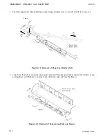
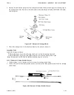
Page 126: ... 5 1 Paper Feed Mechanism Removal 1 Remove the printer mechanism refer to Section 4 2 4 2 Push the notch of the paper guide plate release lever and pull the paper guide release lever and the paper guide release shaft to remove them Figure 4 12 Removal of Paper Guide Plate Release Lever 3 Push the notch of the paper guide plate release lever from the inside of the frame and remove the release lever...

Page 127: ... lift it to remove it Frame Figure 4 14 Removal of Paper Feed Roller Shaft 5 Loosen the four tabs securing the paper guide plate and the paper guide plate spacer to the frame using a screwdriver and lift them to remove them Push the tabs out from the frame Figure 4 15 Removal of Paper Guide Plate and Spacer 4 12 LQ 500 L 1000 ...

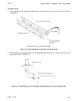
Page 128: ...unt ing direction Viewed from front of printer mechanism Figure 4 16 Paper Guide Plate and Spacer Assembly Points 2 When installing the paper release lever and the paper guide plate release lever carefully observe the mount ing positions shown in Figure 4 17 Figure 4 17 Paper Release Lever and Paper Guide Plate Release Lever Assembly Point LQ 500 L 1000 4 13 ...

Page 129: ...re above 4 2 5 2 Removal of Paper Feed Motor 1 Remove the printer mechanism refer to Section 4 2 4 2 Disconnect the motor cable from the paper feed motor 3 Loosen the tab on the frame which secures the paper feed motor to the frame by pushing it using a screwdriver Remove the paper feed motor by turning it in the direction shown by the arrow below using point A as a fulcrum Viewed from above Viewe...

Page 130: ...Sensor 4 2 5 4 Disassembly of Platen Unit 1 Remove the platen unit refer to Section 4 2 4 1 2 Remove the left shaft holder and the paper feed knob from the platen unit 3 Pull out the platen gear at the right side of the platen unit 4 Remove the E ring from the platen and pull out the right shaft holder and the flat spring Assembly Point When reassembling the platen unit refer to Figure 4 20 to ins...

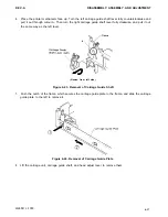
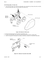
Page 131: ...hat the joint of the carriage unit and the timing belt can be seen through the cutout Figure 4 21 Printer Mechanism Bottom View 4 Detach the timing belt from the carriage unit using round nose pliers Be careful not to damage it 5 Lift portion A of the carriage guide shaft ground plate to remove it from the notch in the carriage motor frame and slide the plate so that it can be removed from the fra...

Page 132: ...ever fully clockwise and pull it out the same way as the left lever Viewed from left side Figure 4 23 Removal of Carriage Guide Shaft 7 Push the notch of the frame which secures the carriage guide plate to the frame and slide the carriage guide plate to the left to remove it Figure 4 24 Removal of Carriage Guide Plate 8 Lift the carriage unit carriage guide shaft and head adjust lever to remove th...

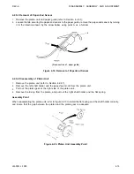
Page 133: ...ad cable pass it correctly through the PFC guide at the frame ADJUSTMENT REQUIRED When the carriage unit is reassembled perform the Platen Gap Adjustment see Section 4 3 1 4 2 5 6 Removal of Carriage Motor 1 Perform steps 1 to 5 of Section 4 2 5 5 2 Disconnect the motor cable from the carriage motor Disconnect the lead wire of the home position sensor from the molded clip at the bottom of the fram...

Page 134: ...ssembly Point Attach the E rings as follows 0 When attaching a ring to the left pulley shaft set it so that its opening faces left 0 When attaching a ring to the right pulley shaft set it so that its opening faces right Using the tweezers confirm that the attached retaining rings do not move 4 2 5 7 Removal of Home Position Sensor 1 Perform steps 1 to 3 of Section 4 2 5 6 to remove the carriage mo...

Page 135: ...t tabs for the ribbon gear cover using a screwdriver At this time just loosen the tabs slightly but do not remove the ribbon gear cover If it is removed before the printer mechanism is turned over the gears will be scattered Bottom view of the printer mechanism Figure 4 29 Ribbon Gear Cover Removal 3 Place the printer mechanism face up and lift the ribbon gear cover to remove it 4 20 LQ 500 L 1000...

Page 136: ... right side covers can be removed at the same time Figure 4 30 Removal of Side Cover 2 Remove the sprocket gear and the sprocket transmission gear 3 4 Remove the shaft holder and remove the sprocket shaft from the sprocket mounting plate Loosen the sprocket mounting plate tab using a screwdriver and pull out the sprocket guide shaft Figure 4 31 Removal of Sprocket Guide Shaft LQ 500 L 1000 4 21 ...

Page 137: ...er guide roller insert the sprocket shaft from the side with the T shaped notch Figure 4 32 Paper Guide Roller Removal and Attachment Assembly Points 1 When attaching the paper guide roller to the sprocket shaft attach it from the direction indicated in Figure 4 32 2 When attaching the sprocket wheel to the sprocket shaft attach it so that the sprocket wheel marks are on the left side and so that ...

Page 138: ... mechanism 3 Remove the printhead then remove the ribbon mask using tweezers When removing the ribbon mask pull it frontward slightly then lift it Figure 4 34 Removal of Ribbon Mask 4 Reinstall the printhead 5 Set the head adjust lever at the position nearest the platen 6 Manually move the carriage to column 10 7 Insert a thickness gauge 0 45 mm between the platen and the printhead and adjust the ...

Page 139: ...p widens Turned counterclockwise The platen gap narrows Turned clockwise The platen gap narrows Turned counterclockwise The platen gap widens Per the form the above adjustment at the 10th and 70th column positions and at the middle of the platen When gaps at all three positions match the adjustment is complete Figure 4 37 Platen Gap Adjustment Positions 4 24 LQ 500 L 1000 ...

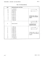
Page 140: ...BMA board or the printer mechanism is replaced 4 3 2 1 Specifications of VR1 and VR2 Bidirectional printing alignment is adjusted by using VR1 and VR2 on the PBMA board VRl is used in draft mode and VR2 is used in LQ mode The specifications of VR1 and VR2 are shown in Tables 4 4 and 4 5 The misalignment usually occurs when the carriage moves from right to left Table 4 4 VR1 Specifications LQ 500 L...

Page 141: ...DISASSEMBLY ASSEMBLY AND ADJUSTMENT Table 4 5 VR2 Specifications REV A 4 26 LQ 500 L 1000 ...

Page 142: ...s the LF switch so that the test pattern is printed The test pattern prints four patterns and the value of the position where VR1 is becomes the center Refer to Figure 4 38 Example VR1 2 Pattern 3 Figure 4 38 Test Pattern Printing Draft Mode 3 Check and select the most aligned pattern 0 If the selected pattern is above the center depress the FF switch an applicable number of times once or twice Re...

Page 143: ...e center Refer to Figure 4 39 Example VR2 9 Pattern 3 Figure 4 39 Test Pattern Printing LQ Mode 3 Check and select the most aligned pattern 0 If the selected pattern is above the center depress the FF switch an applicable number of times once or twice Refer to Table 4 6 0 If the selected pattern is lower than the center depress the LF switch an applicable number of times once or twice Refer to Tab...

Page 144: ... 15 LIST OF FIGURES FIGURE 5 1 FIGURE 5 2 FIGURE 5 3 Troubleshooting Procedure 5 1 Printer Diagnostic System 5 2 Printhead Resistance 5 7 LIST OF TABLES TABLE 5 l TABLE 5 2 TABLE 5 3 TABLE 5 4 TABLE 5 5 TABLE 5 6 TABLE 5 7 TABLE 5 8 Troubleshooting Tools 5 2 Printer Diagnostic System 5 2 Unit Replacement 5 3 Symptom and Reference Pages 5 3 Power Supply Circuit Parts List 5 11 Power Supply Circuit ...

Page 145: ...ypes of problems can occur troubleshooting can be complicated Here is a simple procedure provided to perform troubleshooting Figure 5 1 Troubleshooting Procedures Table 5 1 lists the troubleshooting tools contained in the printer Table 5 1 Troubleshooting Tools LQ 500 L 1000 5 1 ...

Page 146: ...er The host computer sends the test programs to the printer which then executes them The host computer receives the test program results back from the printer and determines the status of the printer Figure 5 2 and Table 5 2 show this diagnostic system Figure 5 2 Printer Diagnostic System Table 5 2 Printer Diagnostic System This system has the following features 0 Provides anyone with a way to tro...

Page 147: ...e unit replacement is based on system analysis According to the particular symptom found by the multimeter the units listed in Table 5 3 need to be replaced Table 5 3 Unit Replacement Numbers Table 5 4 Symptom and Reference Pages LQ 500 L 1000 5 3 ...

Page 148: ...TROUBLESHOOTING REV A 1 Printer Does Not Operate with Power Switch ON 5 4 LQ 500 L 1000 ...

Page 149: ...REV A TROUBLESHOOTING 2 Abnormal Operation of Carriage LQ 500 L 1000 5 5 ...

Page 150: ...TROUBLESHOOTING REV A 3 Incorrect Printing in Self Test with Normal Carriage Operation 5 6 LQ 500 L 1000 ...

Page 151: ...REV A TROUBLESHOOTING Figure 5 3 Printhead Resistance LQ 500 L 1000 5 7 ...

Page 152: ...TROUBLESHOOTING REV A 4 Abnormal Paper Feed with normal printing 5 8 LQ 500 L 1000 ...

Page 153: ...REV A TROUBLESHOOTING 5 Abnormal Operation of Control Panel LQ 500 L 1000 5 9 ...

Page 154: ...TROUBLESHOOTING REV A 6 Incorrect Printing in ON LINE Mode NOTE It is assumed that the host computer operates normally 5 10 LQ 500 L 1000 ...

Page 155: ...ible causes and check points for differences in the power supply circuit The check points include waveforms for normal operation By referring to the checkpoints determine the defective com ponent and perform the proper repair Table 5 6 has the following four columns 0 Symptom Check symptoms against those given in this column 0 Cause Check problems against the causes listed in this column 0 Check P...

Page 156: ...TROUBLESHOOTING REV A Table 5 6 Power Supply Circuit Unit Repair 5 12 LQ 500 L 1000 ...

Page 157: ...REV A T R O U B L E S H O O T I N G ...

Page 158: ... main parts of the control circuit Table 5 7 Control Circuit Parts List 5 3 3 Model 5410 Printer Mechanism Use the diagnostic tool to detect malfunctions among the carriage motor paper feed motor and sensor Table 5 8 lists the specifications for these components Use the printing test and also inspect visually Table 5 8 Device List 5 14 LQ 500 L 1000 ...

Page 159: ...AND ADHESIVE APPLICATION 6 1 LIST OF FIGURES FIGURE 6 1 Correct Adhesive Application 6 2 FIGURE 6 2 LQ 500 L 1000 Lubrication Points 6 3 LIST OF TABLES TABLE 6 1 TABLE 6 2 TABLE 6 3 Lubricants and Adhesive 6 1 Lubrication Points 6 2 Adhesive Application Point 6 2 LQ 500 L 1000 ...

Page 160: ...TION Epson recommends that the printer be lubricated at the points illustrated in Figure 6 2 These lubrication points are listed in Table 6 2 along with the recommended lubricant for each point Epson O 2 or G 27 both of which have been tested extensively and found to comply with the needs of this printer Refer to Table 6 1 for detailed information about O 2 G 19 G 26 and G 27 Be sure that the part...

Page 161: ...MAINTENANCE REV A Table 6 2 Lubrication Points Refer to Figure 6 2 Table 6 3 Adhesive Application Point Refer to Figure 6 1 Figure 6 1 Correct Adhesive Application 6 2 LQ 500 L 1000 ...

Page 162: ...REV A MAINTENANCE Figure 6 2 LQ 500 L 1000 Lubrication Points LQ 500 L 1000 6 3 ...

Page 163: ......

Page 164: ...IGURE A 21 FIGURE A 22 LIST OF FIGURES µPD7810 7811 Pin Diagram A 2 µPD7810 7811 Block Diagram A 3 OP Code Fetch Timing A 6 Memory Read Timing A 6 Memory Write Timing A 6 E01A05KA Pin Diagram A 7 E01A05KA Pin Diagram A 8 E05A02LA Pin Diagram A 10 E05A02LA Block Diagram A 11 HM65256BSP Pin Diagram A 12 HM65256BSP Block Diagram A 12 STK6981B Case Outline Drawing A 13 STK6981 B Functional Equivalent ...

Page 165: ...E A 3 µPD7811 PF Operation A 4 TABLE A 4 µPD7810 PF Operation A 4 TABLE A 5 µPD7810 7811 Port Functions A 5 TABLE A 6 E01A05KA Pin Functions A 9 TABLE A 7 E05A02LA Pin Functions A 11 TABLE A 8 CN2 Connector A 21 TABLE A 9 CN3 Connector A 21 TABLE A 10 CN4 Connector A 21 TABLE A 11 CN5 Connector A 22 TABLE A 12 CN6 Connector A 22 TABLE A 13 CN7 Connector A 22 TABLE A 14 CN8 Connector A 22 TABLE A 1...

Page 166: ... information about the integrated circuits signal functions capabilities etc of components of the LQ 500 L 1000 printer A 1 INTEGRATED CIRCUITS WITHIN THE LQ 500 L 1000 Table A l shows LQ 500 L 1000 ICs Table A l LQ 500 L 1000 ICs LQ 500 L 1000 A l ...

Page 167: ...s 0 8 bit A D converter 0 158 instructions 0 0 8 µs instruction cycle 15 MHz l 16 bit event counter 0 Two 8 bit timer counters 0 3 external and 8 internal interrupts 6 priority levels and 6 interrupt addresses 0 General purpose serial interface asynchronous synchronous and I O modes 0 I O line 7811 40 bit I O port 7810 24 bit edge detection 4 inputs 0 Zero cross detection l Standby function 0 Buil...

Page 168: ......

Page 169: ...APPENDIX REV A Table A 2 µPD7810 Mode Setting Table A 4 µPD7810 PF Operation A 4 LQ 500 L 1000 ...

Page 170: ...REV A APPENDIX Table A 5 µPD7810 7811 Port Functions LQ 500 L 1000 A 5 ...

Page 171: ...s output from T1 T3 fetched at T3 and processed internally at T4 The ALE and RD signals are executed from T1 T3 the OP code fetch for these two signals is performed at T4 The WR signal is output from the middle of T1 to the beginning of T3 The address and ALE timing is the same as that for memory read however following address output AD7 0 PD7 0 are not disabled and write data is output at AD7 0 a...

Page 172: ...s are as follows 1 Parallel I F 2 Address decoder 3 Bank register 4 Data address multiplexer 5 Reset 6 CR motor control Figure A 6 shows the E015KA pin diagram Figure A 7 shows the E015KA block diagram Table A 6 shows pin functions for the E015KA Figure A 6 E01A05KA Pin Diagram LQ 500 L 1000 A 7 ...

Page 173: ...APPENDIX REV A Figure A 7 E01A05KA Block Diagram A 8 LQ 500 L 1000 ...

Page 174: ...REV A Table A 6 E01A05KA Pin Functions APPENDIX LQ 500 L 1000 A 9 ...

Page 175: ...dot matrix printers and is used to simplify the interface between the CPU and the printhead Figure A 8 shows the E05A02LA pin diagram Figure A 9 shows the E05A02LA block diagram Table A 7 shows pin functions for the E05A02LA Figure A 8 E05A02LA Pin Diagram A 10 LQ 500 L 1000 ...

Page 176: ...REV A APPENDIX Figure A 9 E05A02LA Block Diagram Table A 7 E05A02LA Pin Functions LQ 5001 L 1000 A 11 ...

Page 177: ... due to the employment of CMOS peripheral circuits high speed and large capacity as a consequence of its usage of a single transistor memory cell Figure A 10 shows the HM65256BSP pin diagram Figure A l 1 shows the HM65256BSP block diagram Figure A 10 HM65256BSP Pin Diagram A 12 Figure A 11 HM65256BSP Block Diagram LQ 500 L 1000 ...

Page 178: ...olar constant current driving The chopping operation is performed to improve the start up characteristics and minimize heat generation with the constant current The holding terminal included in the STK6981B controls temporary holding Figure A 13 STK6981 B Functional Equivalent Circuit LQ 500 L 1000 A 13 ...

Page 179: ...8C The NJM2355 functions are identical to the TL494 functions It is a pulse width modulation control circuit IC Figure A 14 shows the NJM2355 internal circuit diagram Figure A 14 NJM2355 Internal Circuit Diagram A 14 LQ 5001 L 1000 ...

Page 180: ...ry stable and outputs a large current so that it can replace various Zener diodes It is especially suitable for driving the photodiode in the photocoupler section of the feedback circuit employed in the RCC system switching regulator 0 Temperature compensated reference voltage 50 ppm C TYP 0 High response speed 0 Low noise Figure A 15 TL431CLPB Pin Diagram Figure A 16 TL431CLPB Internal Circuit LQ...

Page 181: ...e internal circuitry of the 74LSO6 hex OC inverter is shown below Figure A 17 74LSO6 Internal Circuit 7407 Hex OC Buffers The illustration below shows the internal circuitry of the 7407 hex OC buffer Figure A 18 7407 Internal Circuit A 16 LQ 500 L 1000 ...

Page 182: ...DIAGRAMS AND SCHEMATICS Figures A 19 through A 30 are exploded assembly and schematic diagrams provided to supplement the text Figure A 19 PEBFIL Board Component Layout Figure A 20 PEBPNL Board Component Layout LQ 5001 L 1000 A 17 ...

Page 183: ...Only F1 2A 125 V 100 V Version 2A 125 V 120 V Version 1 25A 250 V 220 240 V Version PEBFIL BOARD Y566202000 100 V Version Y566202100 120 V Version Y566202200 220 240 V Version Figure A 21 PEBFIL Board Circuit Diagram A 18 LQ 500 L 1000 ...

Page 184: ...REV A APPENDIX PEBPNL BOARD Y566501000 JAPAN ONLY Y566502000 Figure A 22 PEBPNL Board Circuit Diagram LQ 500 L 1000 A 19 ...

Page 185: ...APPENDIX REV A A 20 LQ 500 L 1000 ...

Page 186: ...REV A Table A 8 CN2 Connector Table A 9 CN3 Connector Cont A P P E N D I X LQ 500 L 1000 A 21 ...

Page 187: ...APPENDIX REV A Table A 10 CN4 Connector Cont Table A 12 CN6 Connector Cont A 22 LQ 500 L 1000 ...

Page 188: ...REV A APPENDIX Table A 17 Part No Reference Table LQ 500 L 1000 ...

Page 189: ...APPENDIX REV A Figure A 24 LQ 500 Exploded Diagram A 24 LQ 500 L 1000 ...

Page 190: ...REV A APPENDIX Figure A 25 M5410 Printer Mechanism Exploded Diagram LQ 500 L 1000 A 25 ...

Page 191: ...APPENDIX REV A Figure A 26 Tractor Unit A 26 LQ 500 L 1000 ...

Page 192: ......

Reviews: