background image

 Service Manual

Maintenance

12. When 

the paper is ejected, READY appears 

 the display. Press 

Menu 

once and then press

ALT 

and 

Menu 

together once. TEST MENU appears.

13. Press Item several times until CLEANING 

 appears.

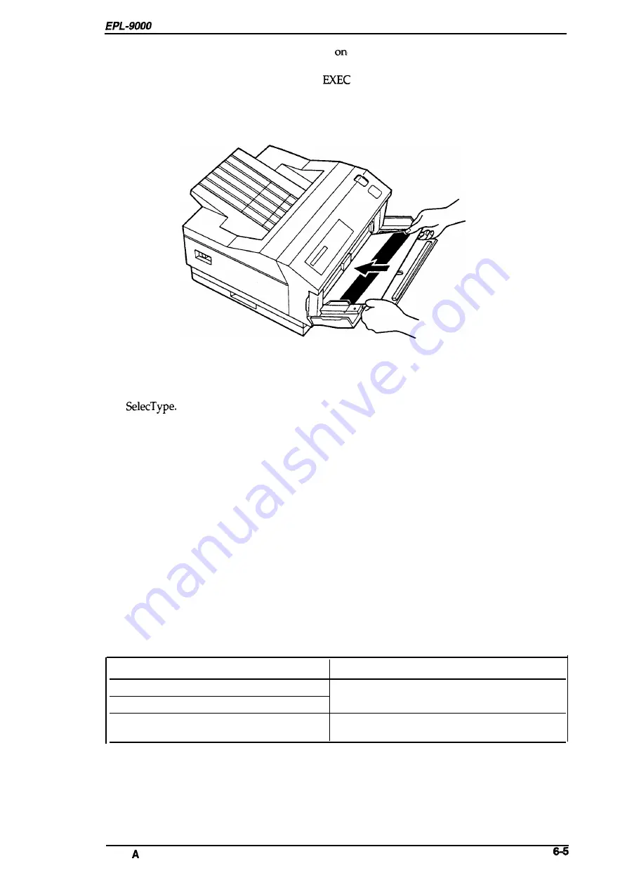
14. Take the same sheet of paper that was printed in Step 11 and insert it into the MSI tray with

the long edge first and the printed side facing up, as shown in Figure 6-8. Then press 

Continue.

Figure 6-8. Imaging Cartridge Replacement (5)

15. The 

paper passes through the printer, cleaning the fusing roller. Then press 

On Line to exit

6.1.2 

Service Maintenance

This section describes the service to be performed by qualified repair personnel.

6.1.2.1 Fusing Unit Service

The 

fusing unit requires periodic service because it is subject to functional deterioration as the total

number of printed pages increases, resulting in bad print quality. The recommend service internal
for the fusing unit is approximately 100,000 pages. This interval is only a suggested value. You do
not need perform service exactly at this interval.
The fusing unit is maintained by cleaning its parts, as described below.

6.1.2.2 Fusing Unit Cleaning

Clean each part 

of the fusing unit using the method specified in Table 6-1. (Refer to Chapter 3 for

disassembly procedures.)

Table 6-1. Fusing Unit Cleaning Procedures

Part 

Name

Cleaning Procedure

Upper fusing roller (in fusing unit)

Lower fusing roller (in fusing unit)

Dip a soft cloth in 

silicon oil and wipe the dust off.

Thermistor (in fusing unit)

Dip a soft cloth in denatured alcohol and wipe the

dust Off .

Rev. 

Summary of Contents for C11C605001 - DFX 9000 B/W Dot-matrix Printer

Page 1: ...EPSON TERMINAL PRINTER EPL 9000 SERVICE MANUAL EPSON ...

Page 2: ...and Epson ESCPare registered trademarks and Epson ESCP2 isa tradernarkof Seiko Epson Corporation Speedo Fontware FaceLift Swiss and Dutch are trademarks of BitStream Inc CG Times and CG Omega are registered trademarks of Miles Inc Univers is a registered trademark of Linotype AG and or its subsidiaries Antique Olive is a trademark of Fonderie Olive Albertus is a trademark of Monotype Corporation p...

Page 3: ...IS MANUAL DO NOT CONNECT THE UNITTOA POWER SOURCE UNTIL INSTRUCTED TO DO SO WHEN THE POWER SUPPLY CABLE MUST BE CONNECTED USE EXTREME CAUTION IN WORKING ON POWER SUPPLY AND OTHER ELECTRONIC COMPONENTS WARNING REPAIRS ON EPSON PRODUCT SHOULD BE PERFORMED ONLY BY AN EPSON CERTIFIED REPAIR TECHNICIAN MAKE CERTAIN THAT THE SOURCE VOLTAGE IS THE SAME AS THE RATED VOLT AGE LISTED ON THE SEIUAL NUMBER RA...

Page 4: ... is 780 nm For Denmark Usem ADVARSEL Usynlig Iaserstri ding ved iibnin n r sikkerhedsafbrydere er ude af funktion Undg5 uds telse for strWng Klasse 1 laser produkt der opfylder IEC825 sikkerheds kravene I For Finland Sweden Users VAROITUS Laitteen lciiyttlhinen muulla kuin t iis sii k t60hjeessa rnainitulla tavalla mat taa altistaa kayttajan turvallisuusluokan 1 ylittavalle nakymattomalI Ia sersii...

Page 5: ...klasse 1 Dette er en halvleder laser Maksimal effeckt til Iaserdiode er 5 mW og brd gelengde er 780 nm Laser Safety Labels Label on rear printer case A laser safety labels is attached on the outside of the printer shown below For Europe lllh r I IASER MASSE 1 NACH IEC 825 CIJLSS 1 IJ SER PRODUCT TO IEC 825 KIA 3SE 1 IJiSER PRODUKT I H T IEC 825 LUOKAN 1 IASER14TE 1 iv ...

Page 6: ...EXPOSIC16N DIREmAAL HAZ VARNING OSYNLIG LAS fRSTRALNING NARDENNA DEL ARoWNADOCH SPARRARARUIWWEADE 5TRALEN AR FARL G AOVARSEL uSYNLIGLASERSTR LING N RDEKSELkWESOG SIKKERHETsLAS 8RYTES UNNG EKSPONERING FoRSTRALEN AOVERSEL USYNLIGLASERSTRAL VEDA8NING NAR SIKKERHEO AF8RYDERE ERUDEAF FUNUTION UNDGAUOSATTELSC FOR TRALING VARO NFWYNEAToN AVA A6w JA SUOIALUKITU5 OHITE1TAES5A OLEIALTTIINA LASERSAIEILYLLE A...

Page 7: ...nd illustrates the main components of the printer CHAPTER 2 OPERATING PRINCIPLES Describes the theory of printer operation CHAPTER 3 DISASSEMBLY AND ASSEMBLY Includes a step by step guide for product disassembly and assembly CHAPTER 4 ADJUSTMENTS Includes a step by step guide for adjustment CHAPTER 5 TROUBLESHOOTING Provides Epson approved techniques for adjustment CHAPTER 6 MAINTENANCE Describes ...

Page 8: ...REVISION SHEET Revision Isaue Date Rev A I Augusl 5 1994 Revision Page I 1s issue I c c vii ...

Page 9: ...TABLE OF CONTENTS CHAPTER 1 CHAPTER 2 CHAPTER 3 CHAPTER 4 CHAPTER 5 CHAPTER 6 APPENDIX GENERAL DESCRIPTION OPERATING PRINCIPLES DISASSEMBLY AND ASSEMBLY ADJUSTMENTS TROUBLESHOOTING MAINTENANCE m Vlll ...

Page 10: ...lTalk Interface 1 19 1 4 OPERATING INSTRUCTIONS 1 20 1 4 1 Control Panel 1 20 1 4 2 SelecType Functions 1 22 1 4 3 Sewice Mode 1 25 1 4 3 1 Hexadecimal Dump Mode 1 25 1 4 3 2 Language Setting Mode 1 25 1 4 3 3 Factory Service Mode 1 26 1 4 3 4 EEPROM Format Mode 1 26 1 4 4 Display ofMessages 1 27 1 4 4 1 Status Messages 1 27 1 4 4 2 Error Messages 1 27 1 4 4 3 Warning Messages 1 28 1 4 5 PrinterSh...

Page 11: ...ard 1 35 Figure 1 18 C8232 k l F Board 1 36 Figure 1 19 Control Panel 1 36 Figure 1 20 MCU PWB Board 1 37 Figure 1 21 LVPS Unit 1 37 Figure 1 22 HVPS Drive 1 38 Figure 1 23 ROS Unit 1 38 Figure 1 24 Fusing Unit 1 39 Figure 1 25 Drive Unit 1 39 Figure 1 26 Imaging Cartridge 1 39 List of Tables Table 1 1 Options for EPL 9000 1 2 Table 1 2 Paper Feed Methods 1 3 Table 1 3 Paper Types 1 4 Table 1 4 Us...

Page 12: ...ology BiRITech r fh the print quality by eliminating jagged edges from images and characters on 600 dpi and 300 dpi printing Optional EPSONScript Level 2 PostScript compatible module EPSON Micro Gray Technology EMGTech which is availabie when using EPSONScript Level 2 mode refines gray scale printing to be comparable to printing on a 12 dpi printer Small and low cost optional LocalTalkTM interface...

Page 13: ...y 8 1 2 4 2 A4 Letter size Yes 8124 250 sheet universal paper tray A3Double Letter size paper A3 Double Letter size tray Yes 81241 Lower paper cassette unit Lower paper cassette unit No include paper cassette Yes 051022 Imaging cartridge Toner cartridge Yes 282326 LocalTalk flF Module Yes 282307M 82a8 32 KB seril interface card Yes 28231 OW 8231 32 KB parallel intetface card Yes 82312X LocalTalkca...

Page 14: ...s Capacity Paper Supply 17 l grj m Paper Size Standard built in paper tray or cassette optional lower A4 Letter paper cassette unit paper cassette I 250 A3 A4 A5 B4 B5 LT HLT LGL EXE GLG B F4 A4 A 5 l T 7 EXE xl L I I IL I Manual feeder MSI M 5 lntemational B5 MON C1O DL C5 Notes 1 The weight in pounds lb is determined weigh 1 g m2 0 2659763 lb 2 The printer can use manual feed for A3 paper by han...

Page 15: ... See Table 1 4 Table 1 4 Usability of Special Paper Input Standard Normal paper paper OHP Envelopes Labefs Card Stock Paper tray R R P N P N Manual feed MSI R R P P P P Envelope cassette N N N P N N R Reliable feeding and good image quality P Possible but better avoided N Not supported Paper size range 98 mm 3 87 inches to 297 mm 11 7 inches Width 140 mm 5 5 inches to 432 mm 17 inches Length Paper...

Page 16: ...C 198 264 VAC Rated frequency range 50 60 Hz Input frequency range 47 63 Hz Power consumption Less than 500 W Less than 600 W 1 2 3 Reliability Specifications MPBF Mean Prints Between Failures Over 12 000 sheets Note MPBF indicates average number of pages printed before occurrence of problem requiring replacement or service Jam rate 1 out of 3 000 sheets or less Standard paper 1 out of 2 000 sheet...

Page 17: ...full storage term Temperature variation must be 10 C 18 F hour or less 20 to 8070 RH over full storage term 5 to RH under extreme conditions Extremes are allowable for up to l 300f full storage term Height 52 cm Vibration frequency 5 to55 Hzand55 to5Hz Acceleration IG Acceleration direction 3 diwction More than 740 hecto pascal 12 months following date of manufacture None EN 60950 IEC950 NEMKO IEC...

Page 18: ...der extreme conditions Extremes are allowable for up to 1 30 of full storage term Temperature variations must be 10 C 18 F hour or less Humidity 20 to 80Y0 RH over full storage term 5 to 95 0 RH under extreme conditions Extremes are allowable for up to 1 30 of full storage term Drop test Height 76 cm 30 4 inches Vibration Same as printer Resistance to atmospheric pressure More than 740 hecto pasca...

Page 19: ...g Available in PCL Switch to PCL ESC OA A Not SUflflOrted supported Reset ESC E Ejects papr and then initialize Ejects paper switches to PCL and then init wlize PJL EJL and ES supported supported Advance Full Page PG AF supported Not SUppIOlted Notes EPSON GL 2 mode has two operational modes One is LJ4 GL 2 mode the other is the GL like rncde LJ4 GL2 mode emulates the GL 2 mode in the HP LaserJet ...

Page 20: ... SWC s NS NS Swiss 742 Bold Italic Condensed SWC s NS NS Incised 901 Swc s NS NS Incised 901 Black SWC s NS NS Incised 901 Italic SWC s NS NS Original Garamond Swc s NS NS Original Garamond Bold SWC s NS NS Original Garamond Italic SWC s NS NS Original Garamond Bold Italic SWC s NS NS Audrey Two Swc s NS NS Flareserif 821 Swc s NS NS Flareserif 821 Extra Bold s NS NS Swiss 721 Roman SWM s s NS Swi...

Page 21: ...BM US IBM DN McText Pchdultilingual VeInternational VeUS PiFont PcE Europe symbol WiAnsi Wingdings ESCIP 2 Mode 15 International characters and 9 code tables USA SPAIN1 FR4NCE JAPAN GERMANY NORWAY UK DENMARK2 DENMARK1 SPAIN2 SWEDENT L AMERICA ITALY KOREAR LEGAL PcUSA 437 PcMu1tilingual 850 PcPortuguese 860 T TPcCanFrench 863 PcNordic 865 PcTurk2 857 PcE Europe 852 BpBRASCII BpAbicomp FX Mode 13 In...

Page 22: ...ter Reverse mode 1 3 1 1 Compatibility Mode of Parallel Interface System STROBE synchronization 8 bit parallel data transfer Handshaking BUSY and ACKNLG signals Connector type P90 25027 1 Amphenol receptacle Applicable plug 57 30360 Arnphenol or equivalent Transfer speed Approximately 400 000 bytes second max Signal timing See Figure 1 3 Signal description See Table 1 8 o 5 o 5 s minimum minimum I...

Page 23: ...signal is specified through SelecType The BUSY signal informs the host computer of the printer state When the sianal is HIGH the minter cannot acceot dat 2 9 DATA 1 8 IN ACKNLG 10 OUT OUT 11 12 BUSY The PE signal indicates paper ernptyfor the standard tray selected through SelecType or command or for the optional PE OUT OUT paper cassett Paper empty is indicated by HIGH Use in reverse mode 13 14 S...

Page 24: ... ACKNLG OUT PtrClk Printer data sending clock 11 BUSY OUT PtrBusy Printer sending data bits 3 and 7 during data transfer to host computer 12 PE OUT AckDataReq Printer sending data bits 2 and 6 during data transfer to host computer 13 SLCT OUT Xflag Printer sending data bits 2 and 6 during data transfer to host computer HostBusy This signal informs the printer of the host computer 14 AUTO FEED IN s...

Page 25: ...face state switch diagram Compatibility Mode r 0 Forward Data ACK and BUSY Transfer SLCT IN HIGH SLCT IN LOW ERR HIGH No data sent ERR LOW I Sending data AUTO FFFD LOW Request to send data AUTO FE ED LOW AUTO FEED HIGH ERR LOW I Figure 1 4 Parallel Interface State Switch Diagram ...

Page 26: ...al is set to HIGH if extension request value was 04h Note3 HB DA Host Busy Data Available HB DNA Host Busy Data Not Available Figure 1 6 shows the data transfer timing chart DATA SEL IN STROBE AUTO FEED ACKNLG BUSY PE SLCT ERROR Peripheral Busy Statu Bit 3 Bit 7 X Peripheral Msy Status Bit 2 Bit 6 N e 1 Bit 1 Bit 5 N e 2 Bit O Bit 4 N te 1 k HB DA Negotiation HB DAor HB DNA Note 3 Figure 1 6 Data ...

Page 27: ...DA Figure 1 7 Termination Timing Note 1 The signal is HIGH when HB DNA The signal is LOW when HB DA Compatibility chart Note 2 The signal is set to HIGH if the extension request value is 03h Note3 Idle LOW Figure 1 8 shows the interrupt tirningchart DATA SEL IN STROBE AUTO FEED ACKNLG BUSY XXXXXX Peripheral Busy status PE c SLCT Note 1 i ERROR u u Reverse Idle Interrupt HB DA Transfer Figure 1 8 I...

Page 28: ...s at HIGH level SPACE and logic 1 is at LOW level MARK 3 RXD RXD IN Serial ASCII data input to the printer It maintains MARK state LOW level between received character codes 4 RTS OUT Transmission request signal output from the printer It is always at HIGH level during power ON 5 CTS IN Always ignored Signal input to the printer The printer can transmit data through TXD while DSR is at 6 DSR IN HI...

Page 29: ... of protocols as listed below and each of them can be designated by SelecType independently DTR DSR protocol SelecType is used to execute the DTR DSR control protocol The DTR signal is set to HIGH when the printer is ready to receive data and to LOW when conditions indicate an error or that the receiving buffer is full When the error is cleared and the printer returns to on line mode the signal re...

Page 30: ...e printer When the DTR signals HIGH the RXD signal can be received by the printer IN The printer transmits the data through TXD while CTS is HIG Serial ASCII data output from the printer HIGH level when SD voltage is higher than SD voltage OUT LOW level when SD voltage is less than SD voltage Logic O is SPACE and logic 1 is MARK state must be maintained between transmitted character codes Ground S...

Page 31: ...d crystal display LCD unit that indicates printer status A variety of printer parameters can be displayed and set using SelecType mode Indicator lights On Line on Communication with the host is possible off Communi tion with the host is not currently possible Flashing This state occurs when the system cannot shift from off line to on line or vice versa Form Feed This LED indicates the data process...

Page 32: ...ars an error Enter to reset operation LCD displays RESET printing stops and the input buffer of current interface is cleared If the RESET button is depressed continuously after RESET is displayed the message displayed on the LCD changes to RESET ALL about 5 seconds and the printer enters to WARM BOOT operation printer clears all RAM Modifies the function of other buttons Enters SelecType mode Chan...

Page 33: ...vailable PITCH 0 44 to 99 99 CPI step 0 01 HEIGHT 4 00 to 999 75 PT Step 0 25 SYMSET Roman 8 ECM94 1 8859 2 ISO 8859 9 ISO IBM US IBM DN PcMuitiiing PcE EuroPs PcTk437 WiAnsi WiE Europe WiTurkish DeskTop PsText Velnternati VeUS MsPuMishin Math 8 PsMath VeMsth PiFont Legal UK ANSI ASCII Swedis2 Italian Spanish German Norwegl French2 Windows FORM 5 to 128 LINES SRC SYMSET o to 3199 DEST SYMS o to 31...

Page 34: ...FF Auto LF ON OFF Zero Char o j Bit Image Dark Light BarCode GL2 GLMODE LJ4GL2 GLIike SCALE OFF AO Al A2 A3 ORIGIN CORNER CENTER PEN 0 1 2 3 4 5 6 END BUIT SQUARE TRIANGULAR ROUND JOIN MITERED MITEREDBEVELED TRIANGULAR ROUND BEVELED NONE PENO 0 05 to 5 00 mm step 0 05 PEN1 0 05 to 5 00 mm step 0 05 PEN2 0 05 to 5 00 mm step 0 05 PEN3 0 05 to 5 00 mm step 0 05 PEN4 0 05 to 5 00 mm step 0 05 PEN5 0 ...

Page 35: ...LG EXE F4 MON C1O DL C5 165 CONFIG MP MODE MANUAL 1ST EXT MP TRAY UNLOCK LOCK STD TRAY UNLOCK LOCK OPT TRAY UNLOCK LOCK SIZE IGNORE OFF ON AUTO CONT OFF ON STANDBY DISABLE ENABLE AUTO SENSE ON PARALLEL SERIAL L T AUX TOP OFFS o to 99 LEIT OFFSET oto150 TONER E F E F E F E F E F TONER LIFE PAGE COUNT o to 99999999 SelecType INIT PARALLEL SPEED FAST SLOW 61 D ON OFF SERIAL SERIAL TYPE RS232C RS422 W...

Page 36: ... 1 4 3 1 Hexadecimal Dump Mode The hexadecimal dump mode is a useful tool in trouble shooting data control problems To enter hexadecimal dump mode turn on the printer while holding down the Form Feed button until HEX DUMP MODE is displayed 1 4 3 2 Language Setting Mode The language setting mode allows the user to specify a language for panel displays and the status sheet To enter language setting ...

Page 37: ...yed veraion Local Language ROM PS ROM EPSONScript Displayed veraion Module ROM PRODUCT PCOUNT Page counter value diaplayed PCOUNT CLEAR Page counter ciear TCOUNT Note 1 TCOUNT CLEAR Toner left counter clear JCOUNT Jam munter value dieplayed JCOUNT CLEAR Jam counter clear With option Note 1 This counter value is leftoftoner weight grarns in imaging cartridge 1 4 3 4 EEPROM Format Mode EEPROM format...

Page 38: ...Error Messages Message Status Measures PAPER JAM A paper jam has occurred Open the cover and remove the jammed paper Then close the cover FEED JAM A paper jam has occurred in the Remove the jammed paper Then feed process press the Continue button PRINTER OPEN Cover is open Close the cover INSERT IMAGING No imaging cartridge Insert the imaging cartridge CRTG INSERT PAPER TRAY No paper cassette Inse...

Page 39: ...while Form Feed Remove cartriige and press light was on or the printer was on line Continue button SERVICE REQ Printer problem SeNice required Xxxxx 1 4 4 3 Warning Mesaages If any of the following warnings occurs it will be displayed on the LCD panel Table 1 16 Warning Messages Message status Measures CHECK PAPER SIZE The paper in the selected tray is Press the Continue button different from the ...

Page 40: ...s printer has two methods of printer sharing port fixed mode and auto sense mode These modes are selected by SelecType menu AUTO SENSE 1 4 5 1 Port Fixed Mode When the printer is in port fixed mode only one interface port is active Data from other ports is ignored Figure 1 10 Port Fixed Mode Memory Rev A 1 29 ...

Page 41: ...ves the data twill print first Mode Assignment ESC P2 mode FX mode User 1 Parallel 4 GL2 mode EpsonScript mode I b Mode Assignment i Vtlal ESCIP2 mode FX mode Auto Sense User 2 t L m w d s 1 EpsonScript mnde Y k r 4 iA Memory Mode Assignment D User 3 ESCIP2 mode I I UT FX mode GL2 mode I B YEpsonScript made t Mode Assignment I ESCIP2 mode AUX FX mode User 4 Input buffer GL2 mode J Figure 1 11 Auto...

Page 42: ...It is able to skip among various destinations as shown in Figure 1 12 The precise specifications for this language are based on the HP LaserJet 4 The figure below shows three types of mode switching Neither EJL nor PJL switches the mode directly They first exit the current mode and return to EJL or PJL Then they enter another mode I LJ4 x I ESCP2 I Figure 1 12 Emulation Switch by SPL 1 4 6 2 Intel...

Page 43: ...I I 1 inch 600 II c When 600 DPI printing Figure 1 14 Effect of BiRITech Note BiRITech is not as effective for printing a mesh pattern or gray scale In such cases BilUTech must be set to OFF The default setting is MEDIUM Since the J3iRlTech effect depends on the toner condition it should be adjusted when the imaging cartridge is replaced or after the imaging cartridge is used for a long time The f...

Page 44: ...B of RAM installed By installing additional SIMMS you can increase the printer s memory to a total of 64 MB including the resident memory EPSON supplies several types of memory option SIMM Other SIMMS can be purchased from other vendors Be sure the SIMM meets the requirements listed below 72 pin type Capacity is one of the following 1 2 4 8 16 32 MB H Access speed is less than 70 ns 9 Within the f...

Page 45: ...controller arcuit board C8232 I F Optkd Optional LocalTalk module Control panel MCU PWB board Engine controller circuit board LVPS unit Low voltage supply arcuit unit HVPS board High vohage supply circuit board ROS unit Optical unit Fusing unit Drive unit Imaging cartridge Housing Paper tray Lower paper cassette unit optional MCU PWB Board C135 MAIN Board LVPS Unit I Control Panel Board c I Drive ...

Page 46: ...ng memory chips and customICS are assigned to the 4 GB memory space H Memory chips Code ROM four 4M bit EP ROM IC5 6 14 13 or two 8M bit mask ROM IC16 15 Font ROM two 8M bit mask ROM M80A76 IC30 M80A77 IC29 4M bit DRAM IC24 25 26 27 16K bit EEPROM IC8 Custom ICS ASIC E05A91 IC7 ASIC E05A92 IC18 ASIC E05A93 IC17 9 Others RS 232C interface driver receiver MAX202 IC19 RS 422 interface driver receiver...

Page 47: ...tion ti Main Chips 85C30 IC3 26LS30 ICI 26LS32 IC2 NJU7660 IC4 26LS30 1 1 NJU7660 IC4 h u I J 1 a 9 1 26LS32 85C30 IC2 C3 Figure 1 78 C8232 l F Board 1 5 3 Control Panel The control panel includes a 20 column x 1 row LCD panel which provides many functions for the printer e g displaying error messages or printer operation status A3600 o n n Elf wp q i on L1l M omIFecII rnw ALT Item A Emu MamJ81 R ...

Page 48: ...hronization laser beam pulse width and power CPU uPD78238 Ul ASIC U2 SMA7029M Figure 1 20 MCU PWB Board 1 5 5 LVPS Unit The LVPS unit is the low voltage supply unit which consists of a switching regulator circuit It converts the AC line voltage into 24V and 5 VDC voltages There are two types of power supply board the 120V type and 220 240V type The difference between the two circuits is only in th...

Page 49: ...VR52 VR51 VR53 VRIO1 I k d R1 no E y Y 3 VR102 figure 1 22 HVPS Board 1 5 7 ROS Unit The ROS unit consists of the laser diode semi conductor laser the mirror motor scanner motor which drives the polygon mirror for laser scannin and several mirrors and lenses The laser beam generated by the laser diode is conducted to the OPC drum surface by way of the polygon mirror as well as several mirrors and ...

Page 50: ...difference between them is the heater lamp Figure 1 24 Fusing Unit 1 5 9 Drive Unit The drive unit consists of the main motor and a series of gears and clutches It drives the paper transport rollers OPC drum sleeve roller fusing roller and some other mechanisms Figure 1 25 Drive Unit 1 5 10 Imaging Cartridge The core mechanisms of the printing process such as charging developing and cleanina are i...

Page 51: ...l Sensor and Exit Sensor Fuser Control Scanner Motor Control LaserDiode Drive Bias Control Fan Motor and Chute Fan Motor Control PaperSize Detection Imaging Cartridge Sensor 2 1 3 10 Power Supply Circuit Function and Safety Protection 2 2 VIDEO CONTROLLER OPERATION 2 2 I C135MAlN Board Operation 2 23 2 2 2 3 2 3 2 4 2 4 2 5 2 5 2 6 2 6 2 7 2 8 2 1o 2 11 2 13 2 14 2 15 2 15 2 16 2 17 2 18 2 19 2 20...

Page 52: ...erExfi Mechanism 2 13 Figure 2 24 Engine Contro er Connecting Diagram 2 14 Figure2 25 Main Motor DfiveCircufi 2 15 Figure 2 26 REGI Sensor and Exfi Sensor OnlOff Timing 2 15 Figure 2 27 Fuser Control Circufi 2 16 Figure 2 28 Temperature for Fuser Control procedure 2 16 Figure 2 29 Scanner Motor Control 2 17 Figure 2 30 Laser Diode Drive Circuti 2 18 Figure 2 31 Bias Control Circuti 2 19 Figure 2 3...

Page 53: ...Trans chute assembly 5 BIAS transfer roll 6 Chute fan M3 7 Fuser assembly 8 Pressure roller 9 Heat roller 10 Exit sensor PC3 11 Thermistor THl 12 Interlock switch 13 Erase lamp assembly 14 Fan M4 15 Raster output scanner 16 CRU SENSOR PWB 17 Main motor Ml 18 Paper cassette 19 Paper size switch SW4 20 Paper out sensor PC1 21 Toner sensor 22 Feed solenoid 23 Feed roller 24 Turn roller 25 Turn soleno...

Page 54: ...2 shows the print process steps and F re 2 3 shows the print process diagram I 1 Drum Charge I v 2 Laser Exposure 3 Development I 4 Image Transfer 1 5 Paper Separation I 6 Fusing I 7 Cleaning 8 Quenching 1 Figure 2 2 Print Process Steps 7 Paper Separatkm 9 Fusing 10 Paper Exit 5 Development 1 Paper Pick up 7 c c Figure 2 3 Print Process Diagram ...

Page 55: ...en 1 Figure 2 4 Drum Charge 2 1 1 2 Laser Exposure Laser exposure is the process of creating an invisible static electricity image on the OPC drum by laser beams emitted from the ROS Raster Output Scanner Assembly The polygon mirror is rotated by the polygon motor scanner motor This is a six sided mirror which rotates in the clockwise direction to produce a laser light scan one side of the mirror ...

Page 56: ...Bias CM Blade L I 1 L Dweloprnent Bias 7 Toner Image Figure 2 6 Development 2 1 1 4 Imsge Trsnsfer Image transfer is the process of transferring the toner image created on the OFC drum in the developing process to paper As the image transfer process this time we have WA the roller image transfer method instead of the corom image transfer In the roller image transfer method there is no generation o...

Page 57: ... 2 1 1 6 Fusing Fusing is the process of fixing the toner image transferred from the image transfer process on the paper This time we have used the heating roller method for fusing The heating roller method is the process of fixing the toner image using the heat roll that is heated by the heater assy When switch on the power the heater assembly lights up until the temperature of the heat roll beco...

Page 58: ...ottle OPC Drum Figure 2 10 Cleaning 2 1 1 8 Quenching After the cleaning process the remaining negative charges on the OPC drum surface need to be eliminated to ensure proper print quality fir the next print During the quentig process the OK drum surface is exposed to the light from the erase lamp to neutralize the OPC drum surface potential c C j Erase Light Lamp OPC Drum c Figure 2 11 Quenching ...

Page 59: ...feed mechanism diagram Paper pick up by feed roll 1 I Paper feed bv turn roll I Paper pick up by pickup roller of pickup roller assembly 1 Paper transpmtation by Upper and Lower REG1 rollof REGI roll assembly 1 J J Paper transportation by OPC drum andBTR Paper transportation by heat roll and pressure roll of fuser J r I Paper exit by exit roll Figure 2 12 Paper Feed Procedure Diagram Heat Roller P...

Page 60: ... paper supply runs out the paper out actuator is lowered causing the shutter to interrupt light from the LED to the photMransistor TM causes the signal to go I DGH informing the engine driver board MCU PWB that the paper cassette is empty The paper cassette of this printer has paper guide plate and paper size detecting cam The paper guide of this cassette m move to fit several size papers This pri...

Page 61: ... time This timing chart is Figure 2 16 I Video l F Signal Paper Position Video Controller Job Total Job Time ISTART h w OPC Drum Feed Rolls REGI Roll Image processing Figure 2 16 Printing Timing Chart 1 This printer fed paper until before registration section before receiving the START signal of engine controller MC PWB so that through put up This printer add PRFD Pre Feed signal of video interfac...

Page 62: ...ons are detected by the MSI sensor located above the pickup rolls While paper is in the MSI the MS actuator for the MSI sensor is lifted When the paper supply runs out the MSI actuator is lowered causing the shutter to intermpt light from the LED to the photo transistor This causes the signal to go HIGH informing the engine driver board MC PWB that the MS is empty REGI I Roll Upper REGI Roil Assem...

Page 63: ...sor After the REGI sensor detects the paper top edge the REGI clutch is turned on and the REGI roll is rotated This time the engine controller MC PWB sends the vertical synchronous TOP Top Of Paper signal to video controller Link Assembly Roil Assembly Trans Chute Assembly 1 Tray Link Retard Pad Figure 2 19 Registration Mechanism 1 REGI MSI Tray L Retard Pad OwerchuteAssemb y u 011 Upper Figure 2 ...

Page 64: ...o fuser by BTR and OPC drum The BTR and OPC drum through paper is vacuumed to trans chute assembly side by air for chute fan Protect of paper jarnming is so that the chute fan vacuum the paper to trans chute assembly side Chute Fan BTR AsS Inlet Chute Solenoid Pick up Rol MSI Sensor 1 Bottom Plate Figure 2 21 Paper Transfer Mechani m c L Rev A 2 12 ...

Page 65: ... fed to the output tray The exit sensor is kxated beyond the pressure roll and the heat roll in the paper path The engine controller MC PWB detects by the exit sensor that paper has been delivered Exit Roller Rod Figure 2 22 Paper Exit Section Pinch Roller Pressure Roller r Figure 2 23 Paper Exit Mechanism Rev A 2 13 ...

Page 66: ...R a 7 Thermal Fuse Scanner Motor D SOB Sensor FEEDER ASSY J 1 c1 CRU SENSOR b Thermistor II t Feed Solencid I L I 1 TURN Solenoid d REG1 Clutch I I i Toner Sensor Not Ued El Paper out Sensor REG1 Sensor I e EXIT Sensor MSI Sensor I _J Paper Size Sensor idcup I Optional 2rrd FEEDER ASSY Solenoid I 7 Chute Fan 1 l J Feed solenoid n Turn Solenoid Detach Saw 1 BTR G s charge We l OPC Drum Paper out Se...

Page 67: ... REGI sensor while paper is feeding This time is long while longer paper is feeding This time is short while shorter paper is feeding One function is paper jam and feed jam detecting to combine for exit sensor If the REGI sensor does not turn on at paper feeding it will be judged feed jam The feed jam is the condition that a paper jam has occurred in the feed process If the following conditions ar...

Page 68: ...HEATER ROD ON signal standby mode fuser temperature is 147 degrees C normal paper printing mode is 152 degrees C and envelope printing mode is 170 degrees C When paper size is set to MONARCFI DL C5 or COM 10 the engine controller board MC PWB sets the fuser temperature to envelope printing mode U PWB ine Controller Board Low Voltage Supply Board LVPS TEMP HEATER ROD ON PIJ11 13 1 AC I AC 1 Fuser P...

Page 69: ...ture of the fusing section rises toanabnormallyhigh level over 220 degrees C and the thermostat did not move 2 1 3 4 Scanner Motor Control Figure 2 29 is the scanner motor control circuit The scanner motor is driving while the scanner motor receives the SCANNER MOTOR ON signal SPI1 and SP12 si als are scanner motor rotating speed setting signals The printing resolution of this printer is 600 DPI d...

Page 70: ...ive Circuit The DATA signal is the laser on off signal When it is LOW the laser is allowed to emit and when it is HIGH the laser is stopped The MO is the laser emission power monitor analog signal The engine controller board MC PWB adjusts the laser emission power by VL2 and VLl signals VL2 and VL1 are laser emission power adjust signals they are analog signals If the signal is not detected it wil...

Page 71: ... signal control to drum charge and DETACH SAW bias While this signal is LOW the DETACH SAW is charged to 1 OK VDC and the OPC drum is charged The imaging cartridge has charged screen between charge wire for OPC drum and OPC drum The charge screen is connected 310 VDC zener diode The charge screen control potential of OPC drum surface to 310 VDC The DB ON signal control to developing bias While thi...

Page 72: ...ntdler board MC PWB during pMtin and the high voltage supply board HVPS sends CHUTE FAN ON signal to chute fan and FAN FASI to fan during printing The fan rotates faster while FAN FAST ON signal receive The chute fan rotates while CHUTE FAN ON signal receive The fan output FAN ALARM signal while it is locked Engine Controller NCUPWS 24 VDC FAN CONTROL FAN AIARM High Voltage y l o x t Front Frame A...

Page 73: ...ssette OFF OFF OFF OFF 0 275 to 0 293 VDC MONARCH OFF OFF OFF ON 0 554 to 0 583 VDC LEGAL 13 I OFF I OFF I ON I OFF I 0 834 to0 871 VDC Japan Post Card OFF OFF ON ON 1 116 to 1 157 VDC COM 10 OFF ON OFF OFF 1 396 to 1 445 VDC LEITER USA ver or OFF ON OFF ON 1 680 to 1 730 VDC A4 Other ver C5 OFF ON ON OFF 1 962 to 2 015 VDC DL OFF ON LEGAL 14 ON OFF EXECUTIVE USA ver or ON OFF B5 Other ver B4 ON O...

Page 74: ...d Figure 2 33 Imaging Cartridge Sensor 2 1 3 10 Power Supply Circuit Function and Safety Protection This printer s low voltage supply board LVPS supplies 5 VDC and 24 VDC The 24 VDC is used bias voltages supply main motor drive polygon scanner motor drive fan motor drive and solenoid drive The 24 VDC line is cut while interlock switch case open switch is off It s a safety protection interlock Low ...

Page 75: ...Operation Figure 2 36 shows a block diagram of the C135 MAIN board The C135 MAIN board contains the video controller which consists of a MB86930 SPARKlite 19 2 MHz 32 bit bus IW3C CPU the standard cells developed for this printer DRAMs ROM and a 16K bit EEPROM CPU M B86930 ICI ROM 16M ROM 16M EEPROM Option IC16 15 or IC8 Board IC5 6 13 14 l 9 30 1 I I J I I JI I I I I A 1 L I T 1 ADDRESS DATA CONT...

Page 76: ...s the folbwing functions Video interface Bi Parallel interface E05A93 ASIC IC17 RS 232C interface 6 RS 422 interface LocalTalk module control Type B interface card control c Control panel control Two 8M ROMs or IC1615 or C5 3 4 These ROMs are code ROM four 4M ROMs Two 8M ROMs iC29 30 These ROMs are font ROM BM ROM IC9 This ROM is local language ROM fonts option This EEPROM stores the fdbwing Model...

Page 77: ... to the engine controller board If such an error occurs the user can increase the V RAM by using SelecType setting PAGE PROTECT The E05A91 transmits image data stored in the V RAM to E05A92 The E05A92 changes image the data format from 32 bits parallel data to serial data and stores it in the internal temporary buffer The temporary buffer has a capaaty equivalent to several lines This is controlle...

Page 78: ... is approximately 128 ms 5V L T WC OUT M51938FP IC23 c 5V 4 RSTIN RSTOUT E05A92 IC18 Figure 2 38 Reset Circuit 2 2 1 2 Bus Control Circuit G The MBS6930 CPU outputs the R W read write signal AS address strobe signal and the BE BE1 BE2 and BE3 signals byteembles to the ASIC EQ5A91 The ASIC E4 5A91 uses these signals to generate the RD read strobe signal WR write strobe signal and READY signal ICI u...

Page 79: ...ss 2 2 1 4 DRAM Management The video controller uses DRAMs for the system RAM and for the V RAM In this printer a standard four 512K x 8 DRAMs are mounted in locations IC24 IC25 IC26 and IC27 providing a total of 2 0 MB SIMM sockets number 1 CN1 and number 2 CN2 are optional SIMM sockets These SIMM sockets can use 1 2 4 8 16 32 MB SIMM 32 bit bus The DRAMs including optional SIMMS are managed by t...

Page 80: ... printer is ready to receive more data from the host computer r ATA b Latch A E05A93 IC17 1 Figure 2 41 Parallel Interface Circuit 2 2 1 6 RS 232C Circuit This circuit uses the RS 232C receiver driver IC MAX202 IC19 to change the signal level horn the RS 232C signal level 12 VDC or 12 VDC to the TI L signal level O V or 5 V or from the TTL signal level to the RS 232C signal level lhis IC converts ...

Page 81: ... I F board It uses three ICS 85C30 IC3 26LS30 ICI and 26LS32 IC2 The 85C30 IC3 changes parallel data to serial data or serial data to parallel data It is controlled by E05A93 IC17 at the C135 MAIN board The 26LS30 IC1 and the 26LS32 IC2 which are signal level change ICS changes a TTL signal level to a LocalTalk signal level compatible with RS 422 signal level Cl 35 MAIN Board E05A93 IC17 CN7 1 0 D...

Page 82: ...e C135 MAIN board and engine controller board can be broadly divided into four groups The first group PRINT CPRDY RDY and PRD gives the status of either the video controller or engine amtmller and indicates whether they are ready to communicate with each other or ready to start the printing operation The second group TOP BD is the synchronizing signal for the printing operation The third group VID...

Page 83: ...3 11 3 2 3 2 Feed Solenoid Removal 3 12 3 2 3 3 Turn Solenoid Removal 3 12 3 2 3 4 Feed Roller Assembly Removal 3 13 3 2 3 5 Feed Roller Removal 3 13 3 2 3 6 Turn Roller Assembiy Removal 3 14 3 2 3 7 Paper out Actuator PESensor Lever Removal 3 14 3 2 3 8 FEEDER PWB Board Removal 3 15 3 2 3 9 Size Spring Removal 3 15 3 2 4 Paper Transpoflation Section Disassembly 3 16 3 2 4 1 3 2 4 2 3 2 4 3 3 2 4 ...

Page 84: ...he Feed Solenoid 312 Figure 3 16 Removing the Tum Solenoid 3 12 Figure 3 17 Removing the Feed Roller Assembly 313 Figure 3 18 Removing the Feed Roller s 313 Figure 3 19 Removing the Tum Roller Assembly 14 Figure 3 20 Removing the Paper out A uator 314 Figure 3 21 Removing the FEEDER PWB Board 315 Figure 3 22 Removing the Size SPrin9 15 Figure 3 23 Removing the Link Assembly s 316 Figure 3 24 Remov...

Page 85: ...emoving the Exit Actuator 3 28 Figure 3 46 Removing the Drive Unit 3 29 Figure 3 47 Removing the CRU SENSOR PWB Board 3 30 Figure 3 48 Removing the Erase Lamp 3 30 Figure 3 49 Removing the ROS Unit 3 32 List of Tables Table 3 1 Tools 3 1 Table 3 2 Screw Abbreviations 3 2 Table 3 3 Screw and Washer Types 3 2 Table 3 4 ChecksafterRepair 3 3 ...

Page 86: ...ing cartridge If the imaging cartridge is removedfiom the printer do not place it in direct sunlight Do not disassemble the optical unit Never turn power on if the optical unit is not installed To prevent damage to ICsfiom static electricity do not touch the ICS on the circuit board or the terminals of peripheral electrical components with your hands Use only the recommended tools to ensure safe a...

Page 87: ...essed Bind head CBB Cross recessed Bind head B tite CBS 0 Cross recessed Bind head S tite with Outside toothed lock washer CP I Cross recessed Pan head I CP S P1 Cross recessed Pan head with Spring lock washer and 1 Plain washer CPFS Cross recessed Pan Flange head S tite Table 3 3 Screw and Washer Types Head Body washer Top Side assembled 1 Gross recessed 1 Eind 1 Normal 1 Plain washer 1 head b 2 ...

Page 88: ...nt Check Point Check Do all LEDs LCD and buttons function normally Does the heater lamp turn on normally Is the test print performed normall I Do cartridge fonts print on font sample printing Does data print in all modes Is it the latest version Are toner and dust removed from the paper path Is the lens on the optical unit clean Is the paper take up roller clean Is the outer surface of the printer...

Page 89: ...ished by performing disassembly in reverse 3 2 1 Housing Removal TMS section describes how to remove the rear top left and right covers 3 2 1 1 Rear Cover Removal 1 Remove the option rnterface cover 2 Rerrwve 1 CBB screw M3 x 8 securing the top cover 3 Remove 1 CB screw M3 x 8 securing the rear cover and remove it Figure 3 1 Removing the Rear Cover 3 2 1 2 Top Cover Removal 1 Remove the rear cover...

Page 90: ...to Section 3 2 l 2 3 Remove 1 CB screw M3 x 8 securing the left cover and remove it Figure 3 3 Removing the Left Cover 3 2 1 4 Right Cover Removal 1 Remove the rear cover Refer to Section 3 2 1 1 2 Remove the top cover Refer to Section 3 2 1 2 3 Remove 1 CB screw M3 x 8 securing the right cover and remove it Figure 3 4 Removing the Right Cover Rev A 3 5 ...

Page 91: ...ove the rear cover Refer to ction32 1 l 2 Remove the top cover Refer to Section 3 2 l 2 3 Remove theleftcover Refer to Section 3 2 13 4 Remove the right cover Refer to Section 3 2 l 4 5 Remove 18 CB screws M3 x 6 securing the shield cover and remove it c3 1 6 7 Figure 3 5 Removing the Shield Cover Dismnnect CN1l and CN12 from the C135 MAIN board Remove 8 CB screws M3 x 6 and 2 CBB screws l x 8 sec...

Page 92: ... 1 to 5 Remove 2 CP screws M3 x 6 securing the font cartridge connector and remove it Remove 3 CP screws M3 x 6 securing the font cartiidge guide and cover and remove them Remove 2 CP screws M3 x 6 securing the option interface cover and remove it Remove the option interface guide Remove 4 CB screws M3 x 6 2 serial interface connector screws and 2 small screws from the rear shield cover and remove...

Page 93: ...Remove 5 CBB screws M3 x 6 securing the engine driver board and remove it Figure 3 8 Removing the MCU PWB Board 3 2 2 4 High Voltage Suppty Board HVPS Board Removal 1 2 3 4 5 6 7 8 Remove the rear cover Refer to Section 3 2 1 1 Remove the top cover Refer to Section 3 2 12 Remove the kftcover Refer to Section 3 2 13 Remove the right cover Ret r to Section 3 2 1 4 Remove the ELEC cover Refer to Sect...

Page 94: ...ll P J12 P J13 P J14 P J15 P J MCU PWB board 6 P J17 P J18 P J19 on the Remove 3 CB screws M3 x 6 securing the MCU box and remove it and the MCU PWB board Remove the fusing unit Refer to Section 3 2 5 1 Figure 3 10 Removing the MCU Box Remove 1 CB screw M3 x 6 securing the earth wire of the HVPS board to the LVPS unit Remove 2 CBB screws M3 x 10 securing the ROS unit and remove connector P101 of t...

Page 95: ...re of the earth plate on the LVPS unit Remove the link assembly Refer to Section 3 2 4 1 Remove 2 CBB screws M3 x 8 securing the earth plate and remove it Figure 3 12 Removing the Earth Plate 3 2 2 7 Fan Unit Removal 1 Remove the rear cover Refer to Section 3 2 l l 2 Remove the top cover Refer to Section 3 2 l 2 3 Remove the leftcover Refer to Section 3 2 13 4 Remove the right cover Refer to Secti...

Page 96: ...3 1 Feeder Assembly Removal 1 Remove the paper cassette and imaging cartridge 2 Turn the left cover over Place the left cover on a SOP cloth so that it will not be damaged 3 Remove 4 CB screws M3 x 8 securing the feeder assembly from the back side and remove it 4 Discomect comector P Jl15 from the FEEDER PWB board PIJ115 Figure 3 14 Removing the Feeder Assembly Rev A 3 11 ...

Page 97: ...EDER PWB board Remove 1 CB saew M3 x 8 securing the feed solenoid and remove it 01 noid Figure 3 15 Removing the Feed Solenoid 3 2 3 3 Turn Solenoid Removal 1 Remove the paper cassette and imaging cartridge 2 Remove the feeder assembly Refer to Section 3 2 3 l 3 Remove 2 CBB saews M3 x 8 securing the feeder tie plate and remove it 4 Remove 2 CBB screws M3 x 8 and 2 CB saews M3 x 8 securing the fee...

Page 98: ...uring the feed housing right and remove it 5 Remove the GEAR IN and GEAR OUT 6 Remove the E ring left securing the feed roller assembly and remove it Figure 3 17 Removing the Feed Roller Assembly 3 2 3 5 Feed Roller Removal 1 Remove the paper cassette and imaging cartridge 2 Remove the feeder assembly Refer to Section 3 2 3 1 3 Push the plastic face of the feed roller while holding the shaft of th...

Page 99: ...ing left securing the turnroller assembly and remove it c Figure 3 19 Removing the Turn Roller Assembly 3 2 3 7 Paper out Actuator PE Sensor Lever Removal 1 Remove the paper cassette and irnagingcartridge 2 Remove the feeder assembly Refer toSection 3 23 1 3 Remove 2 CBB screws M3 x 8 securing the feeder tie plate and remove it 4 Rernove2CBB rews M3x8 and 2 ews x8 securing the feed housing right a...

Page 100: ...M3 x 8 securing the FEEDER PWB board and remove it Disconnect comectors P Jl16 P J201 and P J202 from the FEEDER PWB board Figure 3 21 Removing the FEEDER PWB Board 3 2 3 9 Size Spring Removal 1 Remove the paper cassette and imaging cartridge 2 Remove the feeder assembly Refer to Section 3 2 3 1 3 Remove 2 CBB screws M3 x 8 securing the feeder tie plate and remove it 4 Remove 2 CBB screws M3 x 8 a...

Page 101: ...the front cover unit 5 Remove the shatter lever 6 Remove 2 CBB screws 43 x 8 securing the link assembly and remove it from the ROS unit frame 7 Remove the link assembly while opening the lrnkspring c L y Shatter Lever Figure 3 23 Removing the Link Assembly 3 2 4 2 REGI Roll Assembly Removal 1 open he front cover 2 Disconnect connectors P J26and P J28 from the REGI roll assembly 3 Remove 3 CBB scre...

Page 102: ...EGI roll assembly Refer to Section 3 2 4 2 3 Remove 4 CBB screws M3 x 8 securing the lower chute assembly and remove it Figure 3 25 Removing the Lower Chute Assembly 3 2 4 4 BTR Assembly Removal Never touch the surface of the BTR 1 Open the front cover 2 Remove the BTRassembly Figure 3 26 Removin the BTR Assembly Rev A 3 17 ...

Page 103: ... Remove the ELEC cover Refer to Section 3 2 2 1 Remove the link assembly Refer to Section 3 2 4 1 Disconnect connector P J16 from the MCU PWB board Discomect connector P Jl19 from the EXIT sensor on the fusing unit Discomect comectors P J306 CTR and DS from the HVPSboard Remove 1 CBB screw M3 x 6 securing the earth wire to the front frame Figure 3 27 Removing the Front Cover 1 Remove 2 CBB screws ...

Page 104: ...ard Pad 3 2 4 7 Trans Chute Assembly Removal 1 2 3 4 5 Open the front cover Remove the BTR assembly Refer to Section 3 2 4 4 Disconnect comector P J129 from the chute fan Remove 4 CPFS screws M3 x 10 securing the trans chute assembly Remove 2 CBB screws M3 x 8 securing the wire of the trans chute assembly Figure 3 30 Removing the Trans Chute Assembly ...

Page 105: ... 2 4 9 Pick up Solenoid Removal 1 Remove thetopcover Refer to Section 3 2 1 2 2 Remove theleftcover Refer to Section 3 2 l 3 3 Remove the BTRassembly Refer to Section 3 2 4 4 4 Remove thetrans chute assembly Refer to Section 3 2 4 7 5 Remove thelinkassembly Refer to Section 3 2 4 l 6 Remove 5 CBB screws M3 x 8 securing the front frame assembly to the front rover 7 Remove thepick up roller assembly...

Page 106: ...remove it 8 Discomect connector P J121 from the MSI sensor Figure 3 33 Removing the MSI Sensor 3 2 4 11 Bottom Plate Removal 1 2 3 4 5 6 7 8 Remove the top cover Refer to Section 3 2 1 2 Remove the left cover Refer to Section 3 2 1 3 Remove the BTR assembly Refer to Section 3 2 4 4 Remove the trans chute assembly Refer to Section 3 2 4 7 Remove the link assembly Refer to Section 3 2 4 1 Remove 5 C...

Page 107: ...e trans chute assembly Refer to Section 32 4 7 Remove the link assembly Refer to Section 3 2 4 1 Remove 5 CBB screws hAll x 8 securing the front frame assembly to the front rover Discomect connector P J124 from the control panel and remove the panel while pushing 2 hooks Q k 13gure 3 35 Removing the Control Panel 3 2 4 13 MSI Tray Removal 1 Qen the MSI tray 2 Remove the MSI tray from the left side...

Page 108: ...ng the fusing unit and remove it T Figure 3 37 Removing the Fusing Unit 3 2 5 2 Pressure Roller Removal 1 Remove the top cover Refer to Section 3 2 1 2 2 Remove the fusing unit Refer to Section 3 2 5 l 3 Remove 2 CBB screws M3 x 8 securing the fusing unit top cover and remove it 4 Remove 2 CBB screws M3 x 8 securing the fusing unit cover R and remove it 5 Remove 2 CBB screws M3 x 8 securing the fu...

Page 109: ...op cover and remove it 4 Remove 2 screws securing the exit chute and remove it Figure 3 39 Removing the Exit Chute 3 2 5 4 Exit Roller Removal 1 Remove thetopcover Refer to Section 3 2 l 2 2 Remove the fusing unit Refer to Section 3 2 5 l 3 Remove 2 CBB screws M3 x 8 securing the fusing unit top cover and remove it 4 Remove 2 E rings securing the exit roller and remove it Figure 3 40 Removing the ...

Page 110: ...move 2 CBB screws M3 x 8 securing the fusing unit cover R and remove it Remove 2 CBB screws M3 x 8 securing the fusing unit cover L and remove it Remove the sensor cover and remove 1 CP S P1 saew M3 x 10 securing the thermistor and remove the thermistor Remove 1 CBB screw M3 x 8 securing the earth wire Remove 1 CP S P1 screw M3 x 6 securing connector P JIOl Remove 2 CBB screws M3 x 8 securing come...

Page 111: ...ove 2 CBB screws M3 x 8 securing the fusing unit cover R and remove it Remove 2 CBB screws M3 x 8 securing the fusing unit cover L and remove it Remove the pressure roller Refer to Section 3 2 5 2 Remove the eject chute Refer to Se On 3 25 3 Remove the heater Refer to Section 3 2 5 5 Remove the H R ring securing the right side of the heat roller and remove the H R gear Remove the heat roller along...

Page 112: ... screws M3 x 8 securing the fusing unit top cover and remove it Remove 2 CBB screws M3 x 8 securing the fusing unit cover R and remove it Remove 2 CBB screws M3 x 8 securing the fusing unit cover L and remove it Remove the pressure roller Refer to Section 3 2 5 2 Remove the eject chute Refer to Section 3 2 5 3 Remove the heater Refer to Section 3 2 5 5 Remove the heat roller Refer to Section 3 2 5...

Page 113: ... Remove the exit sensor Figure 344 Removing the Exit Sensor 3 2 5 9 Exit Actuator Removal 1 Remove the top cover Refer to Section 3 2 l 2 2 Remove the fusing unit Refer to Section 3 2 5 l 3 Remove theexit chute Refer to Section 3 2 5 3 4 Remove the exit roller Refer to Section 325 4 5 Remove the exit actuator and spring c 7 Figure 3 45 Removing the Exit Actuator 3 28 Rev A ...

Page 114: ...ove the top cover Refer to Section 3 2 l 2 3 Remove the left cover Refer to Section 3 2 l 3 4 Remove the nghtcover Refer to Section 3 2 l 4 5 Remove the ELEC cover Refer to Section 3 2 2 l 6 Remove the fusing unit Refer to Section 3 2 5 l 7 Discomect connector P J14 from theengine driver board MCUPWB board 8 Remove 3 CBB screws M3 x 29 and 1 CBB screw M3 x 12 securing the drive unit and remove it ...

Page 115: ...to Section 3Q5 1 7 Disconnect connector P Jl18 from the CRU sensor 8 Remove 2 CBB screws M3 x 8 securing the CRU sensor cxwer and move it 9 Remove 2CBBscrews M3 x8 securing the CRU sensor board and remove it Figure 3 47 Removing the CRU SENSOR PWB Board 3 2 6 3 Erase Lamp Removal 1 Remove therear cover Refer to Section 3 2 l l 2 Remove the fusing unit Refer to Section 32S 1 3 Remove 3 CBB screws M...

Page 116: ... 3 Remove theleft cover Refer to ction 3 2 1 3 4 Remove theright cover Refer to Section 3 2 l 4 5 Remove the ELEC cover Refer to Section 3 2 l 5 6 Remove the fusing unit Refer to Section 3 2 5 l 7 Disconnect all comectors from the engine driver MCU PWB board 8 Remove 2 CB screws M3 x 6 securing the MCU box and remove the MCU box and the engine driver MCU PWB board 9 Remove the high vokageu nit Ref...

Page 117: ...Disassembly and Assemb y EPL UXM Service MAnual I T I Figure 3 50 Removing the ROS Unit 3 32 Rev A ...

Page 118: ...Chapter 4 Adjustments No Adjustment is required in this product ...

Page 119: ...R TRAY 5 10 Table 5 17 The LCD Displays SERVICE REQ EOO03 5 10 Table 5 18 The LCD Displays SERVICE REQ EOO05 5 10 Table 5 19 The LCD Displays SERVICE REQ EOO06 5 10 Table 5 20 The LCD Displays SERVICE REQ EOO08 5 11 Table 5 21 The LCD Displays SERVICE REQ EO014 5 11 Table 5 22 The LCD Displays SERVICE REQ COO03 5 11 Table 5 23 The LCD Displays SERVICE REQ COO07 5 11 Table 5 24 The LCD Displays SER...

Page 120: ...r for engine controller and video controller Coool CPU error reserved Video COO02 CPU error privilege violation controller COO03 CPU error illegal instruction error COO04 CPU error no support FPU instruction COO07 CPU error address miss alignment COO09 CPU error reserved Coolo CPU error tag overflow CO017 to 31 CPU error no support interrupt CO036 CPU error no support coprocessor instruction C0128...

Page 121: ...LCD displays ILLEGAL CART 5 9 The LCD displa FEED JAM when using the MSI tray 5 1o FEED JAM The LCD displays FEED JAM when using the standard paper cassette 5 11 The LCD displays FEED JAM when using the optional paper cassette 5 12 The LCD displays PAPER JAM at power 5 13 PAPER JAM The LCD displays PAPER JAM during paper feeding 5 14 NSERT IMAGING CARTRIDGE The LCD displays INSERT IMAGING CARTRIDG...

Page 122: ...be bad Checkpoint Finding Solution Is connector P Jl 1 on the Connect P Jl 1 on MCU PWB board Yes the MCU PWB disconnected board With the power on is there an output of 5 VDC between pin N Replace the LVPS 6 and pin 7 for P Jl 1 on unit the MCU PWB board Replace the MCU PWB board Table 5 4 The Printer Does Not Start RAM Check cause I Step I Checkpoint Finding 1 Solution The video controller board ...

Page 123: ... the No Replace with a guide inserted cartridge supported cartridge The cartridge may be bad 2 Does this printer recognize y Replace the another legal cartridge cartridge l e Cl 35 MAIN board may k 3 Replace the C135 bad MAIN board Table 5 10 The LCD Displays FEED JAM 1 Cause The pick up solenoid coil may be open or shorted step 1 Checkpoint Disconnect connector P J16 on the MCU PWB board and chec...

Page 124: ...ces of all four points approximately 8 The main motor coil may be ohms 2 open or shorted If any coil is shorted check the main motor drive circuit using the following procedure 1 Set the muitimeter to resistance check mode 2 Place the terminal of the multimeter on pins 3 5 4 or 6 of connector Yes Replace the MCU P J14 on the MCU PWB PWB board board 3 Place the terminal of the multimeter on pin 8 o...

Page 125: ...Yes solenoid and the of connector P J201 on FEEDER PWB the FEEDER PWB board board 3 Place the terminal of the multimeter on GND Does the multimeter detect any current Disconnect connector P J202 on the FEEDER PWB board and check the coil resistance between pin 1 and pin 2 on the No Replace the turn disconnected cable side of solenoid the connector using a multirneter Is the resistance approximatel...

Page 126: ...e of the connector using a multimeter Pin 1 Pin 3 Pin 1 Pin 5 Pin 2 Pin 4 Pin 2 Pin 6 Are the resistances of all four points approximately 8 ohms If any coil is shorted check the main motor drive circuit using the following procedure 1 Set the multimeterto resistance check mode 2 Place the terminal of the multimeter on pins 3 5 4 or 6 of connector P J14 on the MCU PWB board 3 Place the terminal on...

Page 127: ... J201 on the FEEDER PWB board 3 Place the terminal of the multimeter on GND Does the muttimeter detect any current D nn connector P J202 on the FEEDER PWB board and check the coil resistance between pin 1 and pin 2 on the disconnected cable side of the connector using a multimeter Is the resistance approximately 220 ohms If the wit is shorted check the solenoid drive circuit using the procedure be...

Page 128: ...rted If any coil is shorted check the main motor drive circuit using the following procedure 1 Set the multimeter to resistance check mode 2 Place the terminal of the muitimeter on pins 3 5 4 or 6 of connector Yes Replace the MCU P J14 on the MCU PWB PWB board board 3 Place the terminal on pin 8 of connector P Jl 1 on the MCU PWB board GND Does the multimeter detect any current The MCU PWB board m...

Page 129: ... The FEEDER PWB Y be 1 Replace the bad FEEDER PWB Table 5 17 The LCD Displays SERVICE REQ EOO03 cause Step Checkpoint Finding Solution The thermistor may be bad 1 Does the LCD display an Yes Replace the error at poweran thermistor The heater lamp may be 2 Check the heater lamp Is it Replace the heater bad OK7 lamp The thermal fuse in the Check the thermal fuse with Replace the fusing unit may be b...

Page 130: ...on The Cl 35 MAIN board may 1 Replace the C135 be bad MAIN board Table 5 24 The LCD Displays SERVICE REQ CIOOO Cause Step Checkpoint Finding Solution The optional SIMM may be Is operation OK after you remove the optional Yes Replace the optional bad SIMM SIMM The C135 MAIN board Y Replace the C135 be bad MAIN board Table 5 25 The LCD Displays SERVICE REQ CII1O Cause Step Checkpoint Finding Solutio...

Page 131: ...5 on the C135 bad MAIN board The Cl 35 MAIN b rd may 2 Replace the C135 be bad MAIN board Table 5 30 The LCD Displays SERVICE REQ C1160 Cause Step Checkpoint Finding Solution ROM IC13 or IC15 on the Is operation OK after Replace ROM IC13 C135 MAIN board maybe 1 you replace the ROM or IC15 on the C135 bad MAIN board The c135 MAIN board may 82 Replace the C135 be bad MAIN board Table 5 31 The LCD Di...

Page 132: ...kpoint Finding Solution Replace the optional interface card Replace the C135 MAIN board Table 5 36 The LCD Displays SERVICE REQ CI31O Cause Step Checkpoint Finding Solution The optional interface card Remove the optional C82312X and LocalTalk VF 1 interface card module C82326X are used C82312X The optional interface card 2 Replace the optional may be bad interface card The C135 MAIN board may 3 Re...

Page 133: ...ti l Opttii unit Check the wi w of C n the i unit is dirty the optical unit Poor image transfer BTR roller Replace the BTR roller Blank print Window of optical o unit is dirty Optical unit Ctean the window n Imaging Replace the imaging Poor Cartridge cartridge development HVPS board Replace the HVPS board Poor image HVPS board Replace the HVPS board transfer BTR roller Replace the BTR roller Black...

Page 134: ...the fusin9 Fusing roller Replace the fusing rfill I En roller roller Paper feed is bad Drive unit Replace the drive unit 31ack line Window of optical Optical unit unit is dirty Clean the window o KI Poor image transfer BTR roller Replace the BTR roller OPC Imaging Replace the imaging RI TER cartridge cartridge Clean the charge wire Improper Charge wire of the imaging charging cartridge Refer to ch...

Page 135: ...n PRINTER OPC Imaging Replace the imaging cartridge cartridge Dirt on the fusing Fusing roller Replace the fusing roller roller Ghost Erase lamp is Erase lamp Replace the erase o bad lamp D Poor image Aj transfer BTR roller Replace the BTR rolie j o n OPC Imaging Replace the imaging fg cartridge cartridge AAA Dirt on the f ing Fining ler Replace the fusing roller roller oggy background Erase lamp ...

Page 136: ... may be bad unit chute unit L Dirt on the fusing Fusing roller Replace the fusing roller roller aper creases Paper cassette Paper cassette Replace the paper o may be bad cassette n Imaging cartridge Imaging Replace the imaging may be bad cartridge cartridge f Trans chute unit Trans chute Replace the trans may be bad unit chute unit Dirt on the fusing Fusing roller Replace the fusing roller roller ...

Page 137: ... Cleaning 6 5 List of Figures Figure6 l lntemal Cleaning 6 1 Figure 6 2 Charge Wire Cleaning 1 6 2 Figure 6 3 Charge Wire Cleaning 2 6 2 Figure 6 4 Imaging Cartridge Replacement 1 6 3 Figure 6 5 Imaging Cartridge Replacement 2 6 3 Figure 6 6 Imaging Cartridge Replacement 3 6 4 Figure 6 7 Imaging Cartridge Replacement 4 6 4 Figure 6 8 Imaging Cartridge Replacement 5 6 5 List of Tables Table 6 l Fus...

Page 138: ...enance performed by qualified repair personnel 6 1 1 User Maintenance Users can achieve maximum print quality from the printer by following the procedures below 6 1 1 1 Cleaning This section describes external cleaning and the cleaning of the optical lens and charge wire for optimal print quality External Cleaning Be sure to disconnect the printer from the power outlet before cleaning Wipe the cov...

Page 139: ...hree layers in the imaging cartridge and the bur slots in the middle layer Clean each slot in the middle layer by pushing the tool into the slot as fir as it will go and moving it several times from side to side as shown in Figure 6 3 c Figure 3 Charge Wire Cleaning 2 4 When you finish cleaning all four slots in the middle layer reinstall the imaging cartridge m the printer 6 2 Rev A ...

Page 140: ...indicating that there is less than 20Y0 of the toner left you should replace the imaging cartridge Imaging Cartridge Replacement 1 Make sure the printer is turned off 2 Gently open the printer cover and remove the imaging cartridge by pulling it towards you 3 Dispose of the used imaging cartridge with non burnable iterns 4 Remove the new imaging cartridge from its aluminum bag While holding the ca...

Page 141: ...P and IUVER FULL appear alternately on the display for about 10 seconds Press Enter while these messages appear READY then appears on the display Note You must press Enter while the WARMING UP and TONER FULL messages appear so 9 10 11 that the TONER option m SelecType will register correctly After READY appears on the display press Menu once and then press ALT and Menu together once TEST MENU then...

Page 142: ...Fusing Unit Service The fusing unit requires periodic service because it is subject to functional deterioration as the total number of printed pages increases resulting in bad print quality The recommend service internal for the fusing unit is approximately 100 000 pages This interval is only a suggested value You do not need perform service exactly at this interval The fusing unit is maintained b...

Page 143: ...ear Side A 19 List of Tables Table A 1 Board Connector Summary A 3 Table A 2 CN1 2 Pin Assignments Table A 3 Table A 4 Table A 5 Table A 6 Table A 7 CN3 Pin Assign ments CN5 Pin Assignments CN6 Pin Assignments CN7 Pin Assignments CN1O Pin Assignments Table A 8 CN11 Pin Assignments Table A 9 CN12 Pin Assignments Table A 10 P Jl 1 Pin Assignments Table A 1 1 P J12 Pin Assignments Table A 12 P J13 Pi...

Page 144: ...ponents Table A 1 gives the size and a description of each connector L HP Font Cartridge CN3 H CN4 Parallel l F 1 Ell Option l F CN5 CN6 EpsonScript Level 2 Board CN7 LocalTalk Module C135 MAIN ml SIMM ml SIMM CN9 Serial l F CN1O CNI1 MCU PWB l I Control Panel CN12 1 LVPS Figure A 1 Cable Connect n for the Video Controller Rev A A 1 ...

Page 145: ...MIS Pul El 1 2 3 4 s 9 7 p P a m U lull p Pus El PU2 Tun 1 F S 24VDC k 1 1 s 24 7 m 24W03 UEO1 C4 U7U V 24WO MO w ToM5ns mol s r MC Nc W Exrrs s 12K O sa Msls r Pla2ws 1 S4mo 1 w I I 24 4 W2 FAF2C 3 TRON 4 m 5 mm MN 7 ON mluo n FANMMW 1 11 OMn 4 77 FAN FA8T 1 Fm Ml 2s M m 4 c s Figure A 2 Cable Connections for the Engine Section 2 Rev A ...

Page 146: ... low voltage supply unit LVPS 14 pins Table A 1 O PIJ12 Connector for ROS unit 13 Dins Table A 1 1 PIJ13 Connector for FEEDER PWB board 12 pins Table A 1 2 P J14 Connector for main motor 6 Dins Table A 1 3 P Jl 5 Connector for HVPS PWB board 11 pins Table A 1 4 P J16 Connector for exit sensor MSI sensor and pick up solenoid pins Table A 1 5 P J17 Connector for REGI clutch toner sensor and REGI sen...

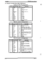
Page 147: ...I o 1 0 o o 0 0 0 o 0 0 0 0 0 o 1 0 Description Ground Data bus bit O Data bus bit 16 Data bus bit 1 Data bus bit 17 Data bus bit 2 Data bus bit 18 Data bus bit 3 Data bus bit 19 5 VDC Not connected Memory address bit O Memory address bit 1 Memory address bit 2 Memory address bit 3 Memory address bit 4 Memory address bit 5 Memory address bit 6 Memory address bl 10 Date bus bit 4 Data bus bit 20 Da...

Page 148: ...ta bus bit 26 55 DQ1l 1 0 Data bus bit 11 56 DQ27 1 0 Data bus bit 27 57 DQ12 1 0 Data bus bit 12 58 DQ28 1 0 Data bus bit 28 59 Vcc 5 VDC 60 DQ29 1 0 Data bus bit 29 61 DQ13 1 0 Data bus bit 13 62 DQ30 1 0 Data bus bit 30 63 DQ14 1 0 Data bus bit 14 64 DQ31 1 0 Data bus bit 31 65 DQ14 1 0 Data bus bit 14 66 NC Not connected 67 Pol Not used 68 P02 Not USf2d 69 P03 Not used 70 P04 Not used 71 NC No...

Page 149: ...data strobe Not connected Font cattridge enable Address bus bit 2 Addrass bus bit 4 Address bus bit 6 Address bus bit 8 Address bus bit 10 Address bus bit 12 Address bus bit 14 Address bus bit 16 Address bus bit 18 Address bus bit 20 Data bus bit 1 Data bus bit 3 Data bus bit 5 Data bus bit 7 Data bus bit 9 Data bus bit 11 Data bus bit 13 Ground 5 VDc Upper data strobe Address decode Ground Addres...

Page 150: ...V TXD READY RXD NC RESET INH CMREQ WRRDY RDREQ WR m E5 GND A3 AO D7 DO 1 0 o 0 i o 0 I I I o 0 0 o 1 0 Description 5 VDC Transmitted data Ready signal Received data Not connected Reset signal l F disabled Request command l F ready Data read request Wriie enable Read enable Chip select Ground Address bus bit 3 O Data bus bit 7 O Rev A A 7 ...

Page 151: ...ss bus bit 2 23 24 GND Ground 25 A5 o Address bus bit 5 26 A6 o Address bus bit 6 27 A3 o Address bus bit 3 28 A4 o Address bus bit 4 29 A9 o Address bus bit 9 30 A1O o Addr bus bit 10 31 A7 o Address bus bit 7 32 A8 o Address bus bit 8 33 A13 o Address bus bit 13 34 A14 o Address bus bit 14 35 Al 1 0 Address bus bit 11 36 A12 o Address bus bit 12 37 A17 o Address bus bit 17 38 A18 o Address bus b...

Page 152: ...Description Read wriie signal Address bus bit 30 Address bus bit 31 Input ready signal Not connected Option select 1 Not connected Read strobe Not connected Clock from CPU Not connected Bomi identification O Board identification 1 Not connected Video clock Reset signal Option select O 5 VDC Initialize signal from the option Video NMI signal TOP signal for video l F Ground Video out Not connected R...

Page 153: ...ables 2 Byte enables 3 Option ready Interrupt request bus bit O Interrupt request bus bit 1 Intemupt request bus bit 2 Ground Interrupt request bus bit 3 CPU ID bit 1 CPU ID bit O Table A 6 CN7 Pin Assignments Signal Name Vcc DTCT m m PCLK IREQ DREQ a m E GND GND ABl DB7 DB6 DB5 DB4 DB3 DB2 DB1 DBO I o I o 0 0 0 0 0 0 0 0 0 o 0 0 I o I o I o I o I o I o I o I o Description 5 VDC Interrupt Norwnask...

Page 154: ...8 GND Ground 19 GND Ground 20 GND Ground Table A 8 CNII Pin Assignments Pin No Signal Name I o Description 1 LCDCLK o System clock 2 PPRDY o LCD data read 3 SWINIT I Switch interrupt 4 GND Ground 5 LCDX o Select of LCD 6 Al I Address bit 1 7 LEDX o LED data wriie 8 SWRDX o Switch data read 9 NC Not connected 10 LCDWRX o LCD data write 11 DBO 1 0 Data bus bit O 12 DB7 1 0 Data bus bit 7 13 DB6 1 0 ...

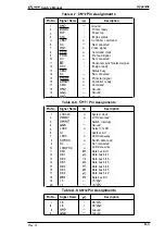
Page 155: ...2 VL1 SG 5VDC SP12 SPI1 SG S M ON RTN 24VDC I o o I o 0 o 0 Description Laser diode dfive data 5 VDc Output level of laser diode Laser diode power adjustment 2 Laser diode power adjustment 1 Ground 5 VDc Scanner motor speed control 2 Scanner motor speed contmi 2 Ground nner motor on Ground 24 VDC Table A 12 P J13 Pin Assignments Signal Name 1 N P 5VDC 2 N P SG 1 P S 2 P S 24VDC 1 T S 2 T S 24VDC 1...

Page 156: ...sfer bias on Transfer bias control Development bias on Ground Drum charge on 24 VDC Fan error signal Not connected Table A 15 P J16 Pin Assignments Signal Name 1 2VDC SG EXIT S 1 2VDC SG MSI S PICK UPS 24VDC NC I o I I o Description Sensor power Ground Exit sensor signal Sensor power Ground MSI sensor signal Pick up solenoid on 24 VDC Not connected Table A 16 P J17 Pin Assignments Pin No Signal Na...

Page 157: ...round 2 Sos I SOS sensor signal 3 5VDC 5 VDc A 1 3 High Voltage Supply Board HVPS Board Table A 19 P J301 Pin Assignments Pin NO Signal Name Description 1 RTN Ground 2 FG Frame ground 3 SCREEN o Screen voltage adjustment 4 DB o Developing bias Table A 20 P J305 Pin Assignments Pin No Signal Nanw m Description 1 FAN FAST o Fan speed control 2 FAN ALARM I Fan error signal 3 24VDC 24 VDC 4 RTN GIound...

Page 158: ...1 r ulwelw LolJl13r4 nIAwl 4W m Imw m UWI13 N a In Ill I I 1A 111111 1 I 1 1 1 1 1 Tl l J JI m Umlcln Unllv u w e 1 I I I I LT 1 I 1111 vOz Uox ul Uoz l uOz OJI N uOx Uox o Voa m z Figure A 4 Control Panel Board Circuit Diagram Rev A 17 ...

Page 159: ...L _ Service Manual A 3 CIRCUIT BOARD COMPONENT LAYOUT I 1 9 6 1 4 7 i UUL l C 4 5 15 IC47 IC46 r l F 1 z 1 1 m i n g 1 5 I c L 3i IJ C36 23 3 7 2 Figure A 5 C135 MAIN Board Component Layout Front Side A 1 8 Rev A ...

Page 160: ...EPL 9000 Service Manual Appendix u C15 0 c 1 c63n R O ns R R39 n al R13 R9 nca o UC31 n R206 mc23 C66CI J Figure A 6 C135 MAIN Board Component Layout Rear Side Rev A A 19 ...

Page 161: ...EPSON ...

Reviews: