
E0C6006 TECHNICAL MANUAL
EPSON
i
CONTENTS
C
ONTENTS
CHAPTER
1 I
NTRODUCTION
____________________________________________ 1
1.1
Features ......................................................................................................... 1
1.2
Block Diagram .............................................................................................. 2
1.3
Pin Layout ..................................................................................................... 3
1.4
Pin Description ............................................................................................. 4
CHAPTER
2 P
OWER
S
UPPLY
AND
I
NITIAL
R
ESET
____________________________ 5
2.1
Power Supply ................................................................................................ 5
2.1.1 Voltage <V
S1
> for oscillation circuit and internal circuits ...................... 5
2.1.2 Voltage <V
L1
–V
L3
> for LCD driving ......................................................... 5
2.2
Initial Reset ................................................................................................... 6
2.2.1 Reset at power-on ....................................................................................... 6
2.2.2 RESET pin .................................................................................................. 6
2.2.3 Oscillation detection circuit ....................................................................... 7
2.2.4 Watchdog timer ........................................................................................... 7
2.2.5 Initialization by initial reset ....................................................................... 7
2.3
Test Input Pin (TEST) ................................................................................... 7
CHAPTER
3 CPU, ROM, RAM ________________________________________ 8
3.1
CPU ............................................................................................................... 8
3.2
ROM .............................................................................................................. 8
3.3
RAM .............................................................................................................. 8
CHAPTER
4 P
ERIPHERAL
C
IRCUITS
AND
O
PERATION
__________________________ 9
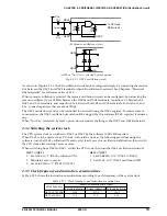
4.1
Memory Map ................................................................................................. 9
4.2
Watchdog Timer ........................................................................................... 11
4.2.1 Configuration of watchdog timer .............................................................. 11
4.2.2 I/O memory of watchdog timer ................................................................. 11
4.2.3 Programming note ..................................................................................... 11
4.3
Oscillation Circuit ....................................................................................... 12
4.3.1 Configuration of oscillation circuit .......................................................... 12
4.3.2 OSC1 oscillation circuit ............................................................................ 12
4.3.3 OSC3 oscillation circuit ............................................................................ 12
4.3.4 Switching the system clock ........................................................................ 13
4.3.5 Clock frequency and instruction execution time ....................................... 13
4.3.6 I/O memory of oscillation circuit .............................................................. 14
4.3.7 Programming notes ................................................................................... 14
4.4
Input Ports (K00–K03, K10–K13) ............................................................... 15
4.4.1 Configuration of input port ....................................................................... 15
4.4.2 Interrupt function ...................................................................................... 15
4.4.3 Mask option ............................................................................................... 16
4.4.4 I/O memory of input port .......................................................................... 16
4.4.5 Programming notes ................................................................................... 17
4.5
Output Ports (R00–R03) .............................................................................. 18
4.5.1 Configuration of output port ..................................................................... 18
4.5.2 Mask option ............................................................................................... 18
4.5.3 Special output ............................................................................................ 19
4.5.4 I/O memory of output ports ....................................................................... 21
4.5.5 Programming note ..................................................................................... 21