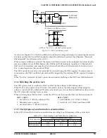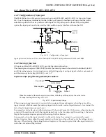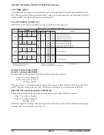
26
EPSON
E0C6006 TECHNICAL MANUAL
CHAPTER 4: PERIPHERAL CIRCUITS AND OPERATION (LCD Driver)
4.7.2 Mask option
(1) Segment allocation
The segment data is decided by the display data written to the display memory at address "0D0H–
0EFH". Writing "1" to the display memory turns the associated LCD segment on, and writing "0" turns
the LCD segment off.
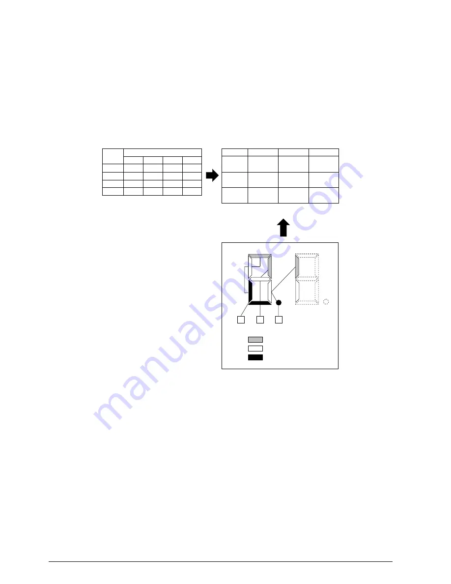
The addresses and bits of the display memory can be made to correspond to the segment terminals
(SEG0–SEG19) in any combination by mask option. This simplifies design by increasing the degree of
freedom with which the liquid crystal panel can be designed.
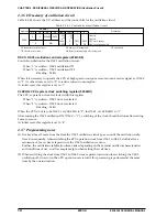
Figure 4.7.2.1 shows an example of the relationship between the LCD segments (on the panel) and the
display memory in the case of 1/3 duty.
a
a'
f
f'
g'
g
e
e'
d
d'
p'
p
c'
b'
b
c
SEG10
SEG11
SEG12
Common 0
Common 1
Common 2
0ECH
0EDH
0EEH
0EFH
Address
d
p
d '
p '
D3
c
g
c '
g '
D2
b
f
b '
f '
D1
a
e
a '
e '
D0
Data
Display memory allocation
SEG10
SEG11
SEG12
E C , D 0
( a )
E C , D 1
( b )
E F , D 1
( f ' )
E D , D 1
( f )
E D , D 2
( g )
E C , D 2
( c )
E D , D 0
( e )
E C , D 3
( d )
E D , D 3
( p )
Pin address allocation
Common 0
Common 1
Common 2
Fig. 4.7.2.1 Segment allocation
(2) Drive duty
Either 1/4 or 1/3 duty can be selected as the LCD drive duty.
4.7.3 Programming note
Because the display memory is for writing only, re-writing the contents with logical instructions (e.g.,
AND, OR, etc.) which come with read-out operations is not possible. To perform bit operations, a buffer
to hold the display data is required on the RAM.


