1
1
2.3.2 Reset Circuit
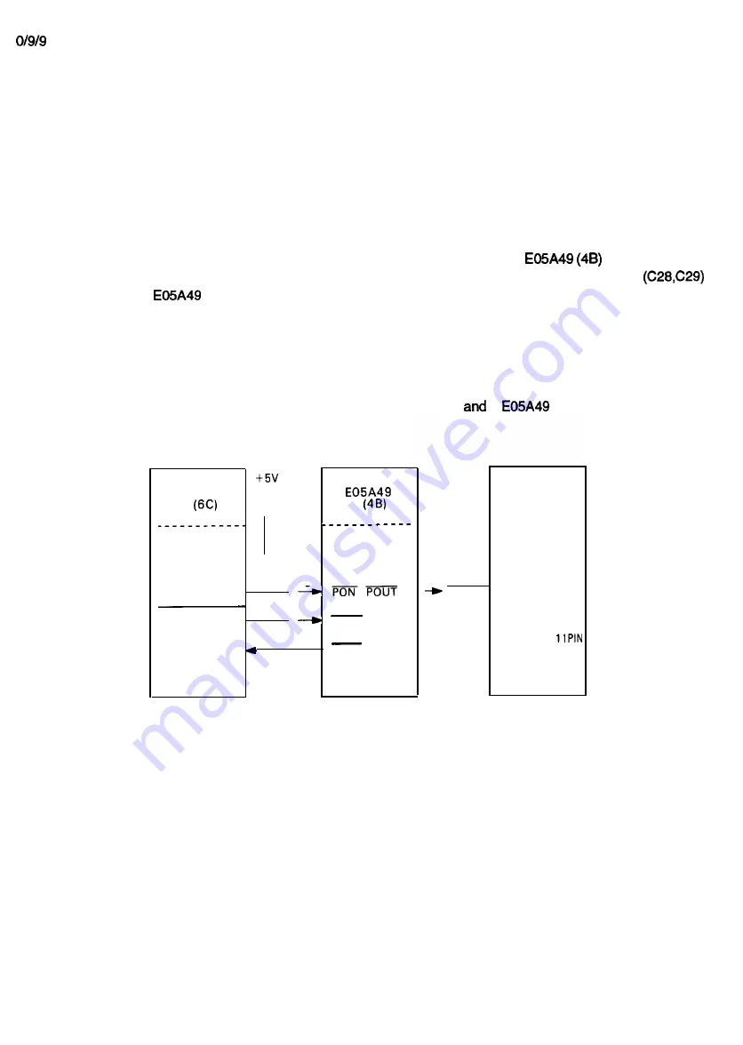
Figure 2-19 shows the reset circuit in block diagram form. The reset circuit issues the /RESET signal. The control
circuits are initialized when they receive the /RESET signal. The conditions under which the /RESET signal is output
are described below.
When you turn on the power
Immediately after you turn on the power, PST-520 (6C) outputs the NCCON pulse.
receives this pulse
and outputs the /DISC pulse.
Then the electrical charge through the resistor (R49) in the condenser
is
discharged. After this,
receives the THLD signal and outputs the /RESET signal. After a certain time has
elapsed, the charge in the condenser builds up again. The THLD signal is canceled and then the /RESET signal is
canceled.
When the CPU performs a reset (CPU self-reset)
The CPU outputs the /RESET signal if there is a /RESET request for E05A49
if
has output the /DISC pulse.
PST520
L i n e
A
1
3
9
OUT
10
T H L D
R69 2K
11
DISC
RESET
CPU RSET 22PIN
OPTION RST
Figure 2-19. Reset Circuit Block Diagram
2-17
Summary of Contents for LQ-1170
Page 1: ...LQ 1170 24 PIN DOT MATRIX PRINTERS TM LQ8 1170 ...
Page 2: ...L Q 8 7 0 1 1 7 0 SERVICE MANUAL EPSON T Printed on recycled paper ...
Page 101: ...10 9 91 Yes NO Replace pluggable chips on main board 5 6 ...
Page 110: ...Table 5 4 Repair of the Power Supply Board Continued 5 15 ...
Page 118: ......
Page 121: ...REV A Figure 6 2 LQ 870 Lubrication Points 6 3 ...
Page 122: ...REV A Figure 6 3 LQ 1170 Lubrication Points 6 4 ...
Page 134: ...1 I II ...
Page 135: ...REV A Q m u D w IL 0 1 xl Figure A 3 CO60 DRV Board Circuit Diagram A 11 ...
Page 136: ...Figure A 4 CO60 PSB Board Circuit Diagram A 12 ...
Page 138: ...LO SLOE002 OWO9 1Nd 0 9 0 3 5 f l P I 11 I 01 I 6 I 8 1 L 9 I 9 I B I I2 I 2 I 1 ...
Page 142: ...REV A Fl 24ov T3 IsA I I II II AL I CU rl Figure A 10 C060 PSE Board Component Layout A 1 8 ...
Page 143: ...LMS d10 IP IMS dla ...
Page 144: ...REV A A 4 EXPLODED DIAGRAM Figure A l 2 1 Exploded Diagram for LQ 870 A 2 0 ...
Page 145: ......
Page 146: ...REV A Figure A 13 1 Exploded Diagram for Model 5DlO A 22 ...
Page 147: ... 5 2 5 610 c 3 5 9 0 El ...
Page 149: ...REV A A 5 CASE OUTLINE DRAWING Figure A l 4 1 Case Outline Drawing for LQ 870 A 25 ...
Page 151: ...lllllll IllI l l IIIIII II0 IIll III1 I I I C O 6 1 M A I N B o a r d A 3 7 ...
Page 152: ... U nRonenl2 i i C O 6 0 HAIN B t _1 m r OL J IIA IS I 19 CNI 36 I I8 I 23 IS ...
Page 153: ...a i iJ 0 E fig tfti I z ...


