background image

L Q - 1 5 0 0

SERVICE MANUAL

EPSON

®

Printed on Recycled Paper

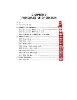
Summary of Contents for LQ-1500

Page 1: ...L Q 1 5 0 0 SERVICE MANUAL EPSON a9Printed on Recycled Paper ...

Page 2: ...ER 3 OPTIONAL EQUIPMENT 3 1 Centronics Compatible Parallel Interface 3 1 3 1 1 Introduction 3 1 3 1 2 Specification 3 1 3 1 3 Operating principal 3 4 3 1 4 Block diagram 3 6 3 1 5 Circuit diagram 3 7 3 1 6 Component layout 3 8 3 2 RS 232C Current Loop Interface 3 9 3 2 1 lntroductron 3 9 3 2 2 Specification 3 9 3 2 3 Operating principal 3 15 3 2 4 Block diagram 3 19 3 2 5 Circuit diagram 3 20 3 2 ...

Page 3: ...t UXMCL 5 18 5 4 Unit Repair Flow Chart UXDRV 5 33 5 5 Unit Repair Flow Chart UXPS 5 40 5 6 Unit Repair Flow Chart IUPIF 5 42 CHAPTER 6 MAINTENANCE 6 1 Maintenance 6 1 1 Cleaning 6 1 2 Inspection 6 2 Lubrication 6 2 1 Lubricants 6 2 2 Lubrication requirement 6 2 3 Lubrication point 6 2 4 Adhesive application requirements 6 2 5 Adhesive application points 6 2 6 Lubricants and adhesives list 6 1 6 1...

Page 4: ...trix Printer Chapters 4 through 6 of the manual deal with the fundamental troubleshoot ing maintenance and repair of the LO 1500 For detail on the disassembly assembly troubleshooting and maintenance of the Model 3660 Printer Mechanism refer to the separately published Techni cal Manual of EPSON Model 3660 The contents of this manual are subject to change without notice Ill ...

Page 5: ...CHAPTER 1 GENERAL 1 1 Product Overview 1 1 1 2 LQ 1500 Interface Overview 1 1 1 3 General Specifications 1 1 1 4 Major Components 1 4 ...

Page 6: ...t loop type serial interface which permits the printer to receive data at a bit rate ranging from 75 to 19200 BPS 3 IEEE 488 Interface An optional interface which permits parallel communication between the printer and any computer or measuring instrument which is equipped with bus structure conforming the IEEE 488 Std 4 8 8 l 9 7 5 1 3 General Specifications 1 Printing Method _ Impact dot matrix 2...

Page 7: ...ting within range 1 step depending on print density 9 Paper Insertion 1 0 Line Spacing 1 1 Print Direction 1 2 Line Feed Repeat Rate 1 3 Ribbon Rear 1 6 1 8 or programmable Bidirectional printing with logical seeking In bit image and double strike mode unidirectional printing from left to right is selected when the power is ON Bidirectional printing is also possible using ESC U 120 ms line when 1 ...

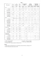
Page 8: ...Table 1 1 3 ...

Page 9: ...LQ 1500 consists of an upper case and lower case The lower case is designed to facilitate mounting of the following components Circuitry for the LQ 1500 is located on five different boards the UXFIL and UXPS PSU 24E boards which house the power supply the UXMCL board which contains most of the control circuitry the UXDRV which handles print mechanism drive circuitry and a interface board IUPIF or ...

Page 10: ...ion One stepper motor operates the print head carriage while the other works as the paper feed motor The Model 3660 is designed to permit easy maintenance Fig 1 2 Model 3660 printer mechanism 3 Contrl circuit boards Fig 1 3 The control circuit is distributed between two circuit boards the UXMCL and UXDRV The UXMCL circuit board performs the central processing and the UXDRV circuit board drives the...

Page 11: ...5 The power supply circuit of the LQ 1500 consists of two major components the UXFIL and UXPS PSU 24E circuit boards Both circuit boards are located in the rear righthand corner The UXPS PSU 24E circuit board supplies DC 24V 12V 12V and 5V to the control circuit and the interface cir cuit Fig 1 5 Power supply circuit board 100 120V version Fig 1 6 Power supply circuit board 220 24OV version 1 6 ...

Page 12: ...it board 2 8 2 3 3 Connector on UXPS PSU 24E circuit board 2 12 2 4 Electrical Circuit 2 13 2 4 1 Power circuit 2 13 2 4 2 Reset circuit 2 22 2 4 3 Sensor circuit 2 22 2 4 4 Carriage motor control circuit 2 26 2 4 5 LF motor control circuit 2 34 2 4 6 Head driver circuit 2 37 2 4 7 Auto sheet load circuit 2 39 2 4 8 Other function 2 40 2 5 Printer Mechanism 2 41 2 5 1 Operation 2 41 ...

Page 13: ...ch major components as printer mechanism control circuits interface circuit power supply circuit and con trol pannel of EPSON LO 1500 Terminal Printer and explains the operating principles of the various me chanism around the electric circuit of the printer 2 2 Connection Diagram Fig 2 1 Fig 2 1 Connection diagram 2 1 ...

Page 14: ...her major LSls include 8255AC5 _ _ _ _ _ _ Output port for head pin drive data 8259A _ _ __ Interrupt controller 8253 5 ___ _ Timer counter 2764 231 28 _ _ _ ___ _ ROM which stores control programs and character patterns uPD41 6 3 _ _ __ RAM which is used as the input data and print data buffer uPB6101 009 _ _ _ Gate array which controls LSls by receiving control signals from CPU Z 80A Fig 2 2 Blo...

Page 15: ...3 1 Connector on UXMCL circuit board 1 Table 2 1 CN1 pin assignment a Use _ Used for data exchange between the main circuit board and the interface circuit board b Number of pins _ _ _ _ _ 50 Table 2 1 Pin assignment CN1 of UXMCL 2 3 ...

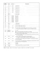
Page 16: ...Note Direction refers to the direction of signal as viewed from the UXMCL circuit board ...

Page 17: ...2 Table 2 2 CN2 pin assignment a Use Data exchange between the main circuit board UXMCL and the driver circuit board UXDRV b Number of pins _ 50 Table 2 2 Pin assignment CN2 of UXMCL 2 5 ...

Page 18: ...2 6 ...

Page 19: ...assignment CN3 of UXMCL Note Direction refers to the direction of signal as viewed from the UXMCL circuit board 4 Table 2 4 CN4 pin assignment a Use _ __ __ _ _ _ _ Signal exchange between the control panel on the UXMCL circuit board b Number of pins _ _ _ 8 Table 2 4 Pin assignment CN4 of UXMCL Note Direction refers to the direction of signal as viewed from the UXMCL circuit board 2 7 ...

Page 20: ...iewed from the UXMCL circuit board 2 3 2 Connector on UXDRV circuit board 1 Table 2 6 CN1 pin assignment a Use _ _ To supply power from the power supply board UXPS PSU 24E to the driver circuit board UXDRV b N u m b e r o f p i n s 4 Table 2 6 Pin assignment CN1 of UXDRV 2 Table 2 7 CN2 pin assignment a Use _ _ _ _ _ _ _ _ Data exchange between the driver circuit board and the Model 3660 printer m...

Page 21: ...Note Direction refers to the direction of signal as viewed from the UXDRV circuit board 2 9 ...

Page 22: ...gnment a U s e Exchange of carriage motor signals between the drive circuit board and the Model 3660 printer mechanism b Number of pins _ 18 Table 2 8 Pin assignment CN4 of UXDRV Note Direction refers to the direction of signal as viewed from the UXDRV circuit board ...

Page 23: ...pins _ _ _ __ 12 Table 2 9 Pin assignment CN5 of UXDRV 6 Table 2 10 CN6 pin assignment a Use _ _ To supply power to the fan set UA from the driver circuit board b Number of pins _ 2 Table 2 10 Pin assignment CN6 of UXDRV 7 Table 2 11 CN7 pin assignment a Use _ _ _ Connectlon of the driver circuit board and the ceramic resistance b N u m b e r o f p i n s 2 Table 2 11 Pin assignment CN7 of UXDRV 2 ...

Page 24: ...CN2 pin assignment Refer to 2 3 1 3 Table 2 3 3 CN3 pin assignment Refer to 2 3 2 1 Table 2 6 4 Table 2 12 CN4 pin assignment a Use ____ __ _ _ _ _ _ _ _ _ _ To supply power from the UXPS PSU 24E circuit board to the fan set UB b Number of pins ___ _ __ _ _ _ _ _ 2 Table 2 12 Pin assignment CN4 of UXPS PSU 24E 2 12 ...

Page 25: ...r supply system in which the input voltage is directly rectified for use Table 2 13 Voltage utilization A 100V 120V version circuit 1 Norse filter circuit 100 120V version Fig 2 3 Noise filter circuit The noise filter circuit IS mounted on the UXFIL board together with the fuse Incoming AC flows through the power switch and fuse before being filtered by a noise suppression circuit on the UXFIL boa...

Page 26: ...harged an excessive charging current that may flow can cause the trouble of fuse F1 or DB1 To prevent it RI limits the inrush current In other words Cl is charged through RI at the time of power on With the start of power supply a voltage is generated at the output of transformer T1 and this is rectified by D11 and thyristor CY1 IS triggered Now the thyristor shorts both the ends of RI thus comple...

Page 27: ...d by R6 and D1 is smoothed by C4 to produce an inverse bias voltage when Q1 or Q2 turns off D3 and D4 are used as the by pass when part of the magnetic energy is returned to the input power D5 and D6 clamp the spike voltage generated by T3 at switching to the DC input voltage via R5 and C20 The clamp voltage is about twice as large as the DC input voltage C21 reduces the transitional switching los...

Page 28: ...te a spike prevention filter 6 Output control circuit 100 120V version Fig 2 8 Output control circuit In this circuit the output voltage is detected and the output is stabilized by controlling the current flowing to the control winding f of VLT The current to the control winding is supplied from e which is the auxiliary power source and is driven by Q3 and Q7 The output voltage is detected by zene...

Page 29: ...DC converter 100 120V version C9 Cll Fig 2 10 DC DC converter circuit In this circuit outputs of 5 I 2 and 12V are produced from 24V This circuit starts oscillating automatically at power on As the base current flows through R31 and Q4 turns on With winding c excited an electromotive force is generated in winding b Q4 turns on quickly because positive feedback of the voltage in winding b is made t...

Page 30: ...D13 which is a two way zener diode clamps the surge voltage generated by T5 to 68V to protect Q4 VR1 is used to set the 5V output voltage 9 5V output circuit 100 120V version 5V output is used for the logic circuit The current flowing through DB3 charges C9 through 11 The extremely large current value however causes a large output voltage ripple which is smoothed by Ls and C12 10 12V output circui...

Page 31: ...ugh the noise filter circuit is rectified at D101 and smoothed at Cl06 and Cl 07 providing the mid point voltage as shown in Fig 2 13 R101 and SCR101 form an inrush current prevention circuit When power is applied the current is charged to C106 and C107 via R101 with SCR101 OFF When the charged voltage rises the converter oscillates SCR101 turns ON and the current path changes from R101 to SCR101 ...

Page 32: ...apable of output control The pulse voltage input to the primary winding terminals 1 and 4 is controlled by the DC current flowing at the control winding terminals 5 and 8 and is output to the secondary winding terminals 9 12 As shown in Fig 2 16 the width of the pulse output to the secondary winding increases as the control cur rent is made larger 2 20 ...

Page 33: ... Vout is maintained at a constant level by a control IC which constantly monitors output and switches transistor Tr301 on or off as required to maintain a constant output The relationship between the input and output voltage is expressed as TON Vout x Vin T 5 Vx PWD Power down circuit 220 24OV version Fig 2 17 Vx PWD circuit This circuit compares the 24V output with the reference voltage to genera...

Page 34: ...n 1 8B and 8A which IS the reset signal port initiator Time constant of the reset pulse is applied at R69 and C4 This time constant is approximately 30 ms Upon the input of an INIT signal from the interface board the interface reset INIT signal is input to the main CPU Z 80A slave CPUs 8042 and 8041 PPI 8255AC 5 gate array uPB6101 009 and timer NE555 The INIT signal is output only during the syste...

Page 35: ...ignal from the phototransistor is integrated and input to the Schmitt circuit which prevents the waveform of the output signal from being disturbed by noise or mechanical vi bra 2 tion MTS sensor circuit Fig 2 20 MTS sensor circuit The MTS sensor circuit detects the signal that defines the speed of the head carriage When the light is screened by the slit plate Fig 2 21 at the photocoupler the phot...

Page 36: ...the output signal from being disturbed by noise or mechanical vibra tion When paper has been inserted in the mechanism the Hall IC is off and pulled up by R63 so that the output of PE signal is LOW When the paper is gone the Hall IC goes on and the collector drops to ground level so that the output of PE signal becmes HIGH The PE signal is applied to T1 pin 39 of CPU8041 A It is possible to render...

Page 37: ...system As the temperature of the print head unit reaches approximately 100 C or above the printing is halted tem porarily and the print head unit IS returned to the home position A thermistor provided in the print head unit is pulled up to 5V As the temperature of the unit rises the re sistance decreases and the voltage at the negative terminal HOT1 HOT2 of the comparator rises higher than the pos...

Page 38: ... the main circuit board The signal is first received by the transistor array and then driven by the regulator IC STK6982 IC2 The 2 2 phase carriage motor runs in combinations of phases A to D See Table 2 14 and Fig 2 25 Fig 2 25 Motor circuit The belt motor sequence for driving the timing belt is shown below 2 26 ...

Page 39: ...Fig 2 26 CR motor drive circuit 2 2 7 ...

Page 40: ...e breakdown or malfunction of the elements To prevent It the energy produced by the counterelectromotive force is released through the zener diode When the output of P22 of 8042 is HIGH the HOLD terminal of STK6982 is HIGH Therefore the common line is cut off from 24V power supply and instead the power is supplied from Vp via the cement resis tances D32 and D33 And the current flows through all th...

Page 41: ...2 15 Motor bias voltage 2 Carriage motor drive signal timing a Acceleration control and constant speed control For acceleration control and contant speed control the following time settings Table 2 16 are available in the printing speed CR motor speed modes of 1 163 pps 769 pps 592 pps and 397 pps Table 2 16 Speed control table 2 29 ...

Page 42: ...Table 2 17 Data of decelerate time ...

Page 43: ...Fig 2 29 Deceleration and stop at home position In case of 1163 769 pps ...

Page 44: ...Fig 2 30 Acceleration and printing control from position other than home position Fig 2 31 Deceleration and stop at home position In case of 1163 769 pps ...

Page 45: ...sition at printer power on is called the home position HP seek The CR motor speeds during the home position seek are all in the 1163 pps mode The following flow chart exemplifies sequence of HP operational events Fig 2 32 Flow chart of home position seek 2 33 ...

Page 46: ...M 1 of the MTS TM where the change of HIGH to LOW of HP signal is recognized and the CR motor is stopped after 18 phase switches h Setting of speed control terminals In each control mode the terminals of 8042 P23 and P24 in the Fig 2 26 must be set as follows Table 2 18 2 4 5 LF motor control circuit Fig 2 34 The control signal of the 4 phase excitation LF motor Fig 2 33 is output from CPU 8041 A ...

Page 47: ... Fig 2 31 shows the time chart for control of the paper feed step motor The control method is a ramp up and ramp down control The time settings for this control are as shown in Table 2 21 This control however is not performed when the amount of paper feed is five steps or less The time set ting at this time is constant speed drive of 4 2 ms per step 4 Paper feed time 3 3 ms 0 l41 mm 100 ms 4 23 mm...

Page 48: ...Fig 2 35 Paper feed timing chart In case of N pulse paper feed N 5 ...

Page 49: ... the out terminal of µPA79C is internally disconnected from the ground and assumes an Open state With the port output of 8255AC5 HIGH the output terminal of µPA79C is internally connected to ground The driving pulse width is determined by the output of pin 1 1 of IC 10C When this output is LOW Q1 is on and the power supply Vx is applied to the base as a pulse to turn on Vcc of uPS79C and the drive...

Page 50: ...ener diode ZD3 provided the current does not flow through the zener diode during the drive And the output of pin 15 of 15C becomes open and is pulled up to 5V by R23 During the non drive time the current flows through the zener diode and the output terminal of pin 15 of 15C is internally connected with ground The output of pin 2 of 14C on the other hand is internally connected to ground during the...

Page 51: ...n paper is present the output of P21 of 8041 goes LOW and the output of pin 10 of IC 15C goes off Since it is pulled up to 5V by R19 Q30 turns on the solenoid is driven and the pa per hold lever is released In this state the PF motor is driven at 510 pulses to execute paper feeding On completion of paper feed CPU 8041 brings P21 to high level Since pin 10 of IC 15C is internally connected to groun...

Page 52: ...o the left end home position in an action of to 0 b Upon receiving print data EPSON for a line the printing is performed in an action of to with the head carriage moving to positior c The CPU receiving the next data analyzes It and determines the acceleration start position of the car riage d In an action of to 0 the carriage is moved to position Then it goes through acceleration printing and dece...

Page 53: ...is illustrated in Fig 2 41 Fig 2 41 Appearance of the printer 2 5 1 Operation 2 5 1 1 Sensor mechanism Signal generating mechanism of Model 3660 The sensor mechanism is composed of an HP home positron sensor an MTS DTS sensor a PE paper end sensor and a print head temperature sensor l The purpose of the HP sensor is to determine the home position of the carriage The sensor generates a reference si...

Page 54: ... the printer is out of paper the magnet touches the Hall IC and generate a signal 4 Print head temperature sensor Two thermistors are built into the print head to detect excessive temperature gains Their resistance value aids in maintaining component compatible operating temperatures 2 5 1 2 Print head assembly The print head unit mounted on the carriage is moved right and left on the carriage sha...

Page 55: ...es out against the platen assembly The dot wire thus pushed out strikes at the platen assembly and prints a dot on the paper through the ribbon On completion of the supply of current to the head driving coil the actuator plate is caused to re turn to its original posltion by the action of the spring By the impact energy and the force of the wire return spring the dot wire is brought back to the or...

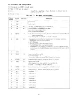
Page 56: ...3 Correspondence between dot wires and FPC terminals Fig 2 45 Printhead connector 2 4 4 ...

Page 57: ...ng 1 Friction feed system for cut sheet Fig 2 47 The paper is held between the platen the paper feeding rollers and the paper holding rollers When the pulse motor rotates the gears constituting a paper feeding gear train are driven in the directions of arrows respectively Consequently the paper is frictionally fed by the platen paper holding rollers and paper feeding rollers in the direction of th...

Page 58: ...he pulse motor rotates the gears in the paper feeding gear train are driven in the directions of arrows respectively Consequently the paper is driven by the sprocket wheels in the direction of the arrow When the tractor feed system is used the paper feeding rollers are held apart from the platen by the action of the release lever Fig 2 47 Tractor sprocket feed mechanism 2 4 6 ...

Page 59: ...ow respectively to disengage the paper holding roller from the platen At this point the pulse motor for paper feeding is driven to feed the paper as specified When the release solenoid is deen ergized the solenoid shaft sub paper holding lever and paper holding lever return to their original positions respectively causing the cut sheet to be pressed against the platen and set for printing Fig 2 48...

Page 60: ...g gear always turns counterclockwise in the next gear train The inked ribbon is housed in the cassette case in an endless state The inked ribbon between the ribbon feeding roller and the ribbon pressure roller is fed when the ribbon feeding roller set in the ribbon driving gear is turned A ribbon braking spring is provided at the exit of the cassette case for preventing the ribbon from losing tens...

Page 61: ...agram 3 19 3 2 5 Circuit diagram 3 20 3 2 6 Component layout 3 21 3 3 IEEE 488 Interface 3 22 3 3 1 Introduction 3 22 3 3 2 Specification 3 22 3 3 3 IEEE 488 operational parameters 3 26 3 3 4 IEEE 488 functional commands 3 27 3 3 5 Block diagram 3 29 3 3 6 Circuit diagram 3 31 3 3 7 Component layout 3 32 3 4 Single Bin Cut Sheet Feeder 8334 Double Bin Cut Sheet Feeder 8344 3 33 3 4 1 Introduction ...

Page 62: ... Transmission 2 Synchronization 3 Handshaking 4 Logic level 8 bit parallel Externally supplied STROBE pulses ACKNLG or BUSY Input data and all interface control signals are TTL compatible 3 1 2 2 Condition setting on the interface board These are two DIP switches on the centronics parallel interface board These switches are set as follows 1 DIP switch setting A DIP 1 Table 3 1 B DIP 2 Table 3 2 No...

Page 63: ...gnment of interface connector A CN1 This connector communicates with CN1 of the UXMCL board Refer to Tab B CN2 Future specification C CN3 This connectorcommunicates with the host computer 1 Number of pins 36 pins Table 3 4 Pin assignment CN3 of IUPIF le 3 1 3 2 ...

Page 64: ...3 3 ...

Page 65: ...be executed without external equipment 3 1 3 Operating principle 3 1 3 1 Data entry As the interface board IUPIF is non buffered a 2 K byte RAM on the main board UXMCL can serve as an input reception buffer This option is selectable via DIP switch setting on the interface board 3 1 3 2 Buffer full empty control Table 3 5 Since signal BUSY is LOW until the 2 K byte input buffer becomes full the dat...

Page 66: ...3 1 3 3 Handshaking of the parallel interface Fig 3 1 Parallel interface timing 3 5 ...

Page 67: ...55AC 5 a programmable peri pheral interface The data bus from the UXMCL board is connected to 8255AC 5 data pin D DT Port B is connected to DIP switches DIP 1 and DIP 2 Ports A and C are used for handshaking with the host com puter As no RAM is incorporated in 8255AC5 interface board IUPIF is non buffered 3 6 ...

Page 68: ...3 1 5 Circuit diagram 3 7 ...

Page 69: ...Fig 3 4 Component layout of IUPIF board ...

Page 70: ...put to the EPSON LQ1500 terminal printer Board components include a CPU and a 2 K byte buffer which has flag control and X ON X OFF control functions Under the interface conditions of RS232C or 20 mA current loop this interface can be applied to asynch ronous serial data transmission systems with a bit rate ranging from 75 to 19 200 BPS under X ON X OFF control or Reverse channel control ...

Page 71: ...hen X OFF 13H signal is sent across pin No 17 and pin No 24 of interface connector Notes 1 The X ON signal is transmitted repeatedly at time intervals after the power switch is turned on 2 LOW and HIGH impedances in current loop are as illustrated below Fig 3 5 Photo coupler 3 About the voltage across pin No 17 and pin No 24 in Current Loop Interface Since the with stand voltage of the photo trans...

Page 72: ...r DIP switches The specifications of DIP 1 and DIP 2 are the same as those on the other interface boards A DIP 1 Refer to 3 1 2 2 B DIP 2 Refer to 3 1 2 2 C DIP 3 Refer to the following table Table 3 8 Setting of DIP 3 Buffer recovery timing DIP 3 3 4 Table 3 9 Buffer recovery timing Vacant area for bytes in the buffer DIP 3 3 3 11 ...

Page 73: ...D DIP 4 Table 3 10 Setting of DIP 4 3 12 ...

Page 74: ...e when RS232C or the current loop in the center machine side is given the power source disconnect J4 J7 Either J8 or J9 must be jump connected ON alternatively Its ON OFF setting differs accord ing to the CPU at delivery Either J10 or J 1 1 must be jump connected ON alternatively With J10 ON as X ON X OFF is transmitted when the reception line of the center machine is open the input buffer may be ...

Page 75: ... B CN2 Future specification C CN3 This connector communicates with the Host Computer 1 Number of pins 25 pin cannon type Table 3 13 Pin assignment CN3 of IURS Notes 1 Direction refers to the direction of signal flow as viewed from the printer 2 All signals except TTY TXD and TTY RXD are based on EIA RS 232C level 3 14 ...

Page 76: ... host computer that data entry is possible b Using current loop The operating principle is the same as for RS 232C However when the 2 K byte buffer is full the impedance between interface connector CN3 pins 17 TTY TXD and 24 TTY TXD R is made HIGH to tell the host computer that the buffer is full When the set value of the buffer recovery timing DIP 3 3 4 corresponds with space available in the buf...

Page 77: ... bytes b When the print processing begins after data entry is prevented the space in the buffer increases gra dually As space remaining in the buffer increases the flag is reset and X ON is transmitted at the preselect ed point timing a b c or d Fig 3 6 Timing a buffer rest space for 152 bytes Timing b buffer rest space for 288 bytes Timing c buffer rest space for 560 bytes Timing d buffer rest sp...

Page 78: ... At the above timing X ON X OFF is transmitted with an interval 80 times the width of one bit cell i e for the data of 10 bits character X ON X OFF is transmitted every 8 characters In addition when the state of X ON X OFF shifts the timing is as follows Fig 3 7 TXD timing in X OFF X ON transition ...

Page 79: ...tor mode data on the RS 232C line are printed in hexadecimal code The timing of Buffer Full Recovery is determined by the DIP switch setting The only difference from the normal processing is that data is printed after it is converted to hexadecimals 3 2 3 4 Miscellaneous function 1 Printer error a Parity error Turning DIP 4 2 ON OFF implements the parity check The check is performed at the CPU for...

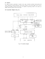
Page 80: ...3 2 4 Block diagram 3 19 ...

Page 81: ...3 2 5 Circuit diagram IURS CIRCUIT BOARD UNIT NO Y49520300000 Fig 3 9 IURS circuit board 3 20 ...

Page 82: ...Fig 3 10 Component layout of IURS board ...

Page 83: ... OV Max 7 Interfacing functions provided The Intelligent IEEE 488 2K buffer Interface Board is provided with the following three operations a AH1 The AH1 allows the printer to receive messages on the DIO lines AH1 includes all the functions of AH The subset of the other required functions is L1 b L1 The L1 provides a device with a function to receive data from another device via the interface This...

Page 84: ...respective func tional settings are as follows Setting of DIP Switches A DIP1 See 3 1 2 2 B DIP2 See 3 1 2 2 C DIP3 Address calculation formula Table 3 16 Setting of DIP SW3 Example The following example shows how to set printer address 6 6 2 4 x O 2 3 x O 2 2 x 1 2 x 1 0 D DIP4 Table 3 17 Setting of DIP 4 Fig 3 11 Setting example 3 23 ...

Page 85: ...lled by setting DIP switch 4 pins 3 and 4 Table 3 18 Once the buffer is full data entry will not be resumed until the buffer can again accommodate the number of bytes desig nated by the switch setting Table 3 18 Setting of DIP SW Pins 4 3 and 4 4 Fig 3 12 Buffer operation 3 2 4 ...

Page 86: ...3 3 2 3 Pin assignment of interface connector A CN 1 Connected to UXMCL circuit board B CN2 Future specification C CN3 Connected to Host Computer 3 25 ...

Page 87: ... is busy Note Pin 4 2 disables the buffer 3 DIP switch 4 2 is ON and the buffer has reached its maximum data capacity See Section 2 Buffer Operation 4 The printer is off line or out of paper Data entry is disabled during periods when the printer is off line or when the paper supply is deplet ed by using one of two switch setting options Setting DIP switch pin 4 6 to ON terminates hand shaking when...

Page 88: ...y two of the IEEE 488 commands are utilized with the IUIE interface board Selected Device Clear SDC which resets the printer and Device Clear DCL which clears the print data stored in the buffer All other commands generally associated with the standard are ignored by the interface board Operation of Inferface to IFC The Interface Clear IFC signal operation mode parameters are set via DIP switch 4 ...

Page 89: ...data line 3 Talker checks NRFD DAV must be LOW NRFD HIGH 4 Listener reads data with DAV LOW NRFD is made LOW for data processing 5 NDAC is made HIGH when listener completes data reception 6 Talker makes DAV HIGH to tell listener that data bus is disabled 7 Listener makes NDAC LOW with DAV HIGH to complete handshake in the state that data is not re ceived 3 28 ...

Page 90: ...3 3 5 Block diagram m x 6 IA 3 29 ...

Page 91: ...ransferred from the IEEE 488 computer or measuring equipment is entered in pPD7811 and then stored in the 2 K byte RAM The stored data is en tered in the buffer on the main board UXMCL The program for data exchange control is stored in the 4 K byte ROM The statuses of DIP 1 2 3 and 4 are each read into memory in the 8255AC 5 or the uPD781 1 at power ON 3 30 ...

Page 92: ...3 3 6 Circuit diagram IUIE CIRCUIT BOARD UNIT N0 Y49520200000 Fig 3 16 IUIE circuit board 3 31 ...

Page 93: ...Fig 3 17 Component layout of IUIE ...

Page 94: ...y feeding paper to the printer one sheet at a time it greatly enhances the speed and effi ciency of letter quality document preparation There are two types of Cut Sheet Feeder a single bin cut sheet feeder 8334 and a double bin cut sheet feeder 8344 Operating principles disassembly assembly and trouble shooting is almost the same This technical manual deals with double bin cut sheet feeder 8344 3 ...

Page 95: ...max 4 Bin capacity Up to 220 sheets of 70 kg paper 80 g m 5 Capacity of paper delivery stand Up to 250 sheets of 70 kg paper 80 g m 6 Environmental condition 1 Temperature Operation 5 to 35 C Rate of change should not exceed 8 C hour Storage 30 C to 65 C Non condensation 2 Humidity Operation 20 to 80 Non condensation Storage 5 to 85 Non condensation 7 Reliability 1 MCBF Mean Cycle Between Failure ...

Page 96: ... paper properly Cut sheet paper a b C d e Paper weight 52 kg paper 60 g m 86 kg paper 100 g m Tolerance Paper width tolerance 0 5 mm 0 020 Paper must be cut squarely go with a deviation of less than O O3 Paper type and quality Paper used should be plain bond typewriter quality paper with light wood pulp content Paper should have no wrinkles or other visible defects Storage conditions Temperature 1...

Page 97: ...quirements The cut sheet feeder is a mechanical device which is controlled by printer platen movement The complete drive and select mechanism is located on the right hand side frame Both side frames are protected by detachable molded plastic covers which are cover the mechanical components The feed bin supports have two locking positions 0 Operating position In this position the paper in the bin i...

Page 98: ...feeder it will be transported into the output stacker The eject roller shafts are permanently driven by platen motion in forward direction This keeps the paper tight against the platen When the paper is under platen control the eject rollers slip on the surface of the paper because the fric tion between the platen pinch rollers and the platen is much stronger than the friction between the cut shee...

Page 99: ...tion of the shafts 0 The eject roller shafts are only driven to transport a form into the output stacker The pressure of the brake levers prevents uncontrolled motion of the catch plates The catch plate is a part of the selection and feed unit 3 4 3 5 Operating the paper bins Fig 3 20 Left side of the feeder With the left hand side release lever the paper bin can be opened for stacking paper When ...

Page 100: ...ing piece position at the drive wheel defines the home position of the catch plate The select mechanism of the catch plate consists of the home position keeper and the turnout spring Fig 3 21 Construction of the selection and feed unit 1 Operation of the selection and feed unit The operation of the selection and feed unit can be divided into three main cycles a Home Position Cycle Printer platen m...

Page 101: ...e following schematic diagrams and their associated descriptions the three main operation cycles are described in detail The term motion direction is based on the motion direction of the printer platen a Home Position Cycle a The home position keeper rests on the engaging piece of the catch plate Drive wheel and catch plate will rotate synch ronously in a forward direction Rotation of the drive wh...

Page 102: ... by applied platen mo tion to the corresponding pick up roller shaft Carry out of n line spaces in reverse direction inserts a single sheet until it rests on the platen with a slight bow in the paper This bow creates a constant pressure of the sheet being inserted against the platen friction rollers When n 34 Bin 1 Red one is selected n 52 Bin 2 Blue one is selected 0 When all drive wheels are dri...

Page 103: ...er body before starting disassembly or assembly 2 Avoid loosening screws other than those specified 3 For safety the operator should wear glove 3 4 4 1 Disassembly The procedure for disassembling the cut sheet feeder 8334 8344 is described in this section 1 a Removal of the basket stacker paper stand side cover bottom pan and foot Paper stands Fig 3 27 Removal of the stacker paper stands Hold the ...

Page 104: ...he bot tom Set the release lever free and open the pawl on the botton outward The side cover will then come off The pawls are positioned at the points shown in the drawing Fig 3 30 Removal of the side cover Bottom view of the sheet feeder d Removal of the bottom pan The bottom pan is simply inserted along the groove from the rear side It can be removed by pulling outward as shown in the following ...

Page 105: ...n the single bin cut sheet feeder and four in the double bin cut sheet feeder The paper guide is symmetrical and can be removed in the same way Pull the release lever to the side and secure the pressure shaft a Remove left and right pressure plates The pressure plates are mounted so that bin 1 is at the front and bin 2 at the rear the ribs engage with the pickup roller Disengage the pressure plate...

Page 106: ...p to disengage the pawl and then lift it up with the screwdriver blade Fig 3 34 Removal of clamp c Remove Paper Guide from the Frame Remove the paper guide from the frame by moving the paper guide at an angle to the front Disengage the retaining arm from the frame push the arm forward and remove the paper guide Caution If you try to remove the paper guide from the frame with the retaining arm enga...

Page 107: ...ad wider than the circumference of the hole in the brake lever Use a pair of pliers to pinch the peg inward so that the levers can be slipped over it Brake lever Fig 3 37 Removal of brake lever c Removal of selection and feed units 1 and 2 There are two bin selectors the red unit operates bin 1 the blue unit operates bin 2 Each unit can be removed by taking out one E ring and pulling outward from ...

Page 108: ...he pickup roller first pull the pickup roller to the left and take out the right shaft then lift it out Fig 3 40 Removal of pickup roller 4 Removal of the pressure shaft Remove the E ring attached to the gear of either the left or right side and take the pressure shaft out of the frame Fig 3 41 Removal of the pressure shaft 3 47 ...

Page 109: ...al of output selector arms c Remove left and right screws securing profile 0 and remove the profile d To remove the front eject roller shaft 0 grasp the left and right side and pull forward e Remove the output selector 0 Fig 3 43 Removal of profile eject roller shaft output selector f Release the plastic tabs at either side of the rear eject roller shaft then grasp the shaft at each end and pull f...

Page 110: ...he gear wheel attached to the printer adapter right side is secured with the snap in type gear lock Pry the gear lock off with a flat bladed screw driver Fig 3 45 Removal of the printer adapter right gear wheels 3 4 4 2 Assembly The procedure for assembling the cut sheet feeder 8334 8344 is described in this section The proce dure is basically the reverse to that for disassemby Some points requiri...

Page 111: ...mounted by letting it rest in the rear position on the rail Fig 3 47 The red rings on the pressure shaft are designed for facilitating movement of wider paper or paper placed in a horizontal position through the platen assembly The rings are interchangeable and may be replaced facing in either direction 3 Mounting the pickup roller gear wheel selection and feed units 1 and 2 and brake levers a b T...

Page 112: ...es and Pressure Plates For mounting the paper guides and pressure plate pull the release lever to the front and secure the pres sure shaft First mount the left and right paper guides of bin 2 rear position and then the left and right pressure plates Next mount the left and right paper guides of bin 1 front position and the left and right pressure plates Notes 1 If the mounting order is wrong the l...

Page 113: ...sembly 3 4 5 2 Troubleshooting procedure The troubleshooting procedure following consists of a two part check of component functions The first step is to evaluate whether malfunction is caused by incorrect assembly the second step is to see whether the probelem may be traced to a defective component Caution Remove the cut sheet feeder from the printer before performing any repair procedure Note So...

Page 114: ... Checking operation of the whole unit Check operation by manual operation with the Cut Sheet Feeder mounted on the printer 3 53 ...

Page 115: ...3 54 ...

Page 116: ...3 55 ...

Page 117: ... Fault of selection and feed 3 56 ...

Page 118: ... Fault of paper guides1 3 57 ...

Page 119: ... Fault of output selector 3 58 ...

Page 120: ... Other faults Paper is fed at an angle 3 59 ...

Page 121: ...ar ried out by the operator after suitable instruction Intervals are determined by the operating time and the paper type being used Paper dust accumulation varies with the quality of the paper 3 4 6 2 Tools and gages required Brush soft Platen cleaner MULTIPLI Fedron Platen Cleaner Cloth lint free Vacuum cleaner Precautions l We recommend platen cleaner MULTIPLI or its equivalent as cleaning agent...

Page 122: ...f one of the pick up rollers is damaged or unevenly worn both rollers must be replaced Caution Regularly check the pick up roller shafts the eject roller shafts and the gear wheels for wear or da mage Clean the following three parts as necessary 0 Clean the DELRIN bushes of the eject roller shaft with denatured alcohol l Clean the studs of all gear wheels with denatured alcohol 0 Check the functio...

Page 123: ......

Page 124: ...ism 4 6 4 3 4 Removal of fan set UB head cooling fan 4 6 4 3 5 Removal installation and adjustmnent of print head 4 7 4 3 6 Removal of CPU and ROM 4 9 4 3 7 Adjustment of print alignment backlash 4 10 4 4 Adjustment 4 12 4 4 1 MTS and DTS sensor board adjustment 4 12 4 4 2 H P sensor board adjustment 4 14 4 4 3 Backlash of the carriage motor and belt driving pulley 4 15 4 4 4 Backlash of the paper...

Page 125: ...les 4 1 and 4 2 of this section must be prepared by the user prior to disassembling and troubleshooting the LQ 1500 Under the column Class in Table 4 2 code A denotes the tool or measuring instrument mandaton for maintenance and repair of the printer whereas code B denotes the tool or measuring instrument not necessarily essential but recommended to facilitate such maintenance and repair Table 4 1...

Page 126: ...ssembled component can be reassembled by reversing the disassembly process Therefore assembly procedure is omitted 4 3 1 Removal of upper case Fig 4 1 To check the inside of the LQ 1500 first open the upper case according to the procedure below STEP 1 Remove the accessories such as the printer lid sheet guide etc STEP 2 Remove the hand paper feed knob STEP 3 Remove 6 screws from the upper case Fig...

Page 127: ...UIE or IURS The procedure for removing these boards described below should be followed when even replacing a cir cuit part 1 Removal of control circuit board UXMCL The control circuit board on which many parts are provided is the center of the electric circuit boards Removal work should be carried out with care in the following procedure STEP 1 Remove the upper case See paragraph 4 3 1 STEP 2 Remo...

Page 128: ...oval of driver circuit board UXDRV The driver circuit board drives the head carriage and paper feed assemblies STEP 1 Remove the upper case See paragraph 4 3 1 STEP 2 Disconnect the connectors from the driver circuit board 1 Disconnect connector CN2 0 2 Disconnect connector CN3 0 3 Disconnect connector CN4 0 4 Disconnect connector CN5 0 5 Disconnect connector CN7 0 6 Disconnect connector CN6 0 STE...

Page 129: ...se See paragraph 4 3 1 STEP 2 Disconnect the connectors from the power circuit board 1 Disconnect connector CN3 0 2 Disconnect connector CN2 0 3 Disconnect connector CN4 0 STEP 3 Remove screw from the GND terminal in the AC inlet STEP 4 Remove 3 screws securing the power circuit board to the base plate Fig 4 6 Removal of the UXP UXFIL board Fig 4 7 Removal of the I F unit 4 5 ...

Page 130: ... 0 2 Disconnect connector CN4 0 3 Disconnect connector CN5 0 STEP 3 Disconnect connector CN5 from the control circuit board UXMCL STEP 4 Remove four screws securing the mechanism to the lower case Fig 4 8 Removal of the M 3660 printer mechanism STEP 5 Lift the mechanism then remove it 4 3 4 Removal of fan set UB head cooling fan STEP 1 Remove the upper case See paragraph 4 3 1 STEP 2 Remove the pr...

Page 131: ...head STEP 2 Manually the print head fully to the left STEP 3 Holding the head connector section down disconnect the connectors in order first the right then the left with the head cables kept in a horizontal position Fig 4 10 Removal of head cable STEP 4 Remove the print head by removing 2 screws 0 securing it Fig 4 11 Removal of print head STEP 5 Remove the ribbon mask Note Pull up the ribbon mas...

Page 132: ...ws STEP 3 Connect 2 head cables to the connectors on Model 3660 in order from left to right Caution Unless head cables are securely connected the assembly may not function STEP 4 Adjust the opening between the print head top and the platen to approximately 0 5 mm and tighten the 2 screws Fig 4 13 Gap adjustment Note Insert the thickness gauge laterally 4 8 ...

Page 133: ...1 To remove a circuit board follow the removal procedure in paragraph 4 3 2 STEP 2 Remove the ROM and RAM from the board with care 1 When replacing ROM 1 1 Using a chip extractor remove the chip If extractor is not available carefully un plug the chip gradually loosening it 1 2 To replace the ROM insert it in its socket matching the index points notches which indicates pin 1 on the chip and socket...

Page 134: ...ch SW1 Fig 4 15 Location of SW1 2 Position and function of SW1 1 SW1 1 SW1 2 Table 4 3 below defines the results of each switch setting combination when the print direction is right to left in the low speed printing mode Table 4 3 Setting of SW1 1 SW1 2 Table 4 4 below defines the results of each switch setting combination when the print direction in the right and left Table 4 4 Setting of SW1 3 S...

Page 135: ...he printing backlash when the print alignment on one line becomes bad This ad justment is performed by starting the test program of ROM with the operation of dip switch SW1 Please adjust step by step according to the following flow chart 4 11 ...

Page 136: ...ne side of resistance R35 on the UXMCL board TIME 200 uset Note Resistance R35 is near the IC 5C Turn off Dip switch 2 7 on the interface board so that it is in DRAFT mode Set the paper and execute self print test Check the following waveform Fig 4 16 MTS If the waveform is not the same as above go to stop 10 If the waveform is same as above then skip to STEP 13 Loosen the setscrew CP P M2 5 x 4 o...

Page 137: ... signal is same as above timing adjustment is correct STEP 16 Loosen the setscrew CP P M2 5 x 4 of the DTS sensor board STEP 17 Move the DTS sensor board in the direction of the arrow to adjust T2 cycle to be almost equal for both travel courses Standard value of T2 cycle for both travel courses Within 20 us Fig 4 19 Adjustment of the DTS sensor position STEP 18 Securely tighten the setscrew STEP ...

Page 138: ... H characters STEP 3 Loosen the setscrew CP P M3 x 6 of the H P sensor board STEP 4 Move the H P sensor board in the direction of the arrow and align so that the scale shaft graduations comes to the center of the letter If adjustment has been completed Go to step 5 Note Turn the switch to off each time and adjust STEP 5 Confirm the phase of MTS and DTS signals when this adjustment has been perform...

Page 139: ...arriage motor and belt driving pulley Fig 4 24 If print alignment with both directional print is bad adjust the backlash STEP 1 Loosen the setscrews CPO M3 x 6 which tighten the carriage motor frame and carriage motor mounting plate STEP 2 Adjust the backlash between the motor pinion of the carriage motor and the belt driving pulley Standard value 0 05 to 0 15 mm 1 Adjust the backlash by moving th...

Page 140: ...ed motor Adjust the backlash between the motor pinion of the pulse motor and the paper feeding re duction gear Standard value 0 05 to 0 15 mm 1 Adjust the backlash by the paper feeding reduction gear 2 Confirm the backlash at three points during one rotation of the paper feeding reduc tion gear STEP 3 Securely tighten the setscrews CPO M3 x 6 Fig 4 25 Backlash of the paper feed motor 4 16 ...

Page 141: ...HOOTING 5 1 Entry of Troubleshooting 5 1 5 2 Check out Procedure 5 4 5 3 Unit Repair Flow Chart UXMCL 5 18 5 4 Unit Repair Flow Chart UXDRV 5 33 5 5 Unit Repair Flow Chart IUPIF 5 40 5 6 Unit Repair Flow Chart UXPS 5 42 ...

Page 142: ...Use The check out procedure provides entry to repair for troubles whose nature is not clear enough Level Repair is made by unit replacement Those with basic knowledge of machinery can per form this repair 2 Unit repair flow charts Use The flow charts guide you to the repair of a faulty unit on the component level Level Repair is made on the component level so that it requires a high level of mecha...

Page 143: ...The user is recommended to keep the following replacement components Circuit boards Electric devices 5 2 ...

Page 144: ... Mechanical components Model 3660 Y450590100 Maintenance tool 5 3 ...

Page 145: ...5 2 Check out Procedure Repair by Unit Replacement 5 4 ...

Page 146: ...5 5 ...

Page 147: ...5 6 ...

Page 148: ...5 7 ...

Page 149: ... Carriage does not return to home position when power switch is turned on 5 8 ...

Page 150: ... Carriage does not move ...

Page 151: ...5 10 ...

Page 152: ... Control panel indication is faulty Paper feeding motor does not stop 5 11 ...

Page 153: ... Switch on control panel can operate in the on line state 5 12 ...

Page 154: ... Sheet loading does not work properly ...

Page 155: ... LF and FF switches does not operate in off line state Carriage does not move in Self Printing Test 1 5 14 ...

Page 156: ... Carriage does not move in Self Printing Test 2 5 15 ...

Page 157: ... Paper feeding is not made in Self Printing Test Printing is faulty 5 16 ...

Page 158: ... Operation is abnormal when connected with host computer 5 17 ...

Page 159: ...5 3 Unit Repair Flow Chart UXMCL 5 18 ...

Page 160: ...1 Printing Troubles 5 19 ...

Page 161: ...5 20 ...

Page 162: ... ...

Page 163: ...5 22 ...

Page 164: ...5 23 ...

Page 165: ...2 Carriage Troubles 5 24 ...

Page 166: ...5 25 ...

Page 167: ...5 26 ...

Page 168: ...5 27 ...

Page 169: ...5 28 ...

Page 170: ...3 Paper Feeding Troubles 5 29 ...

Page 171: ...5 30 ...

Page 172: ...5 31 ...

Page 173: ...4 Sheet Loading Problem 5 32 ...

Page 174: ...5 4 Unit Repair Flow Chat t UXDRV 5 33 ...

Page 175: ...1 Printing Troubles 5 34 ...

Page 176: ...5 35 ...

Page 177: ...2 Carriage Troubles 5 36 ...

Page 178: ...3 Paper Feeding Troubles 5 37 ...

Page 179: ...5 38 ...

Page 180: ...4 Sheet Loading Troubles 5 39 ...

Page 181: ...5 5 Unit Repair Flow Chart IUPIF 5 40 ...

Page 182: ...5 41 ...

Page 183: ...5 6 Unit Repair Flow Chart UXPS 5 4 2 ...

Page 184: ... 24 voltage is not output The malfunction of the primary 5 43 ...

Page 185: ...on check to see whether the converter which connects the D C power supply 10 to 30V to A C input oscillates inter mittently If it oscillates the power supply of the primary circuit func tions correctly If after making this check the problem is not isolated follow the steps in flow chart 1 1 then turn the power on again 5 44 ...

Page 186: ...The voltage of 24 is low Excessive voltage is output 5 45 ...

Page 187: ... 5 is abnormal 5 46 ...

Page 188: ...Vx is abnormal 12 is abnormal 5 47 ...

Page 189: ...ning 6 1 6 1 2 Inspection 6 1 6 2 Lubrication 6 2 6 2 1 Lubricants 6 2 6 2 2 Lubrication requirement 6 2 6 2 3 Lubrication point 6 2 6 2 4 Adhesive application requirements 6 3 6 2 5 Adhesive application points 6 3 6 2 6 Lubricants and adhesives list 6 4 ...

Page 190: ...inter As part of his routine work the operator should check if the printer is properly used and see to it that the printer may serve in the best condition 0 Check points Check if the paper is not caught around or by the paper feed box the printer casing or other objects Check if the cassette ribbon is set in position see Fig 2 1 Check if dusts or other foreign materials are not found in the printe...

Page 191: ...sembled or its parts are replaced be sure to lubricate irrespec tive of the time set for periodic lubrication A Every six months or each time 1 000 000 lines have been printed B Every occasion of overhaul or each time 5 000 000 lines have been printed 6 2 3 Lubrication points Refer to Lubrication and Adhesive Application Points Drawing For 1 to I 0 lubrication is necessary while assembling Ref Lub...

Page 192: ... tions During disassembly reassembly or parts replacement apply adhesive to the required points according to the list below or Lubrication and Adhesive Application Points Drawing The adhesive to be used for the printer is Neji Lock Green 2 6 2 5 Adhesive application points Refer to Lubrication and Adhesive Application Points Drawing 6 3 ...

Page 193: ...parts due to flow of adhe sive so pay attention to application quantity See Fig 6 1 Fig 6 1 6 2 6 Lubricants and adhesives list The lubricants and adhesives which are indipensable for maintenance and repair are given below 0 Commercially available 0 Available only from EPSON 6 4 ...

Page 194: ...d adhesive application points drawing B 7 37 Lubrication and adhesive application points drawing C 7 38 UXMCL circuit diagram 7 39 Component layout of UXMCL board 7 40 UXDRV circuit diagram 7 41 Component layout of UXDRV board 7 42 UXPS circuit diagram 7 43 Component layout of UXPS board 7 44 PSU 24E circuit diagram 7 45 Component layout of PSU 24E board 7 46 UXFIL circuit diagram 7 47 ...

Page 195: ...List of Principal lC s Table 7 1 7 1 ...

Page 196: ...rray of this memory The array is formed of 16 8 bit registers and 4 16 bit registers any of which is a static RAM Two sets of 6 general purpose registers a total of 12 registers are provided on the chip Each regis ter can be used as a single 8 bit register or paired to form a 16 bit register Other registers on the chip include 2 sets of accumulators and 2 sets of flag registers Main resister set S...

Page 197: ...s register 1 The Z 80 CPU has a mode in which indirect call indirect subroutine jump can be applied to any memory location according to the interruption For this purpose register I is provided The contents of this register refer to the 8 high order indirect address bits The address which meets the equipment which has applied an interruption is assigned to the 8 low order bits In this system the in...

Page 198: ...able for a wide range of applications When a simple read write memory is needed for a simple program and especially in a ROM based sys tem it is advisable to substitute general purpose registers for it 1 2 Arithmetic logic unit ALU The 8 bit arithmetic logical operation instruction is executed at the ALU inside the CPU The ALU is connected to each register through the internal bus to perform data ...

Page 199: ...bits Tri state I O active HIGH Do D7 forms an 8 bit two way data bus The data bus is used for data ex change with memory or I O unit or between them Output active LOW Machine cycle 1 MREQ Memory request Signal Ml is emitted when the current machine cycle is the OP code fetch cy cle of an instruction execution It should be noted that when executing a 2 byte OP code signal MI is emitted at every fet...

Page 200: ...MREQ when the refresh address for dynamic memory is on the low order 7 bits of the address bus Output active LOW Signal HALT is emitted when the CPU has executed a HALT instruction and re quires a maskable mask enabled or non maskable interrupt before resuming operation During HALT time the CPU maintains memory refresh by executing NOPs Input active LOW This input signal tells the CPU that memory ...

Page 201: ...ut active LOW With RESET input the program counter comes to zero and the CPU is initia lized At this time the following state is entered 1 Interruption enable flag is reset 2 Register I is set to 00H 3 Register R is set to 00H 4 Interruption is set to mode 0 During reset the address bus and data bus have HIGH impedance so that all control outputs become inactive BUSRQ Input active LOW Bus request ...

Page 202: ...a memory or an I O unit This M cycle also consists basically of 3 to 5 cycles However the cycle number changes with the wait sig nal which is input to synchronize with an external unit An explanation on the timing in a basic machine cycle is given below Fig 7 3 All CPU timings are analyzed as shown in Fig 7 4 simplified timing chart The respective basic oper ation timing charts with and without th...

Page 203: ...t on the data bus from any other memory segment Signal MREQ during refresh time is used to read the data for refreshing all dynamic memories The re fresh signal cannot be used alone The reason is that since the refresh address is stable only while signal MREQ is emitted the two signals must be used together Fig 7 5 represents the delay of the fetch cycle when the wait signal WAIT is incuded The CP...

Page 204: ...be used for the memory read write pulse directly In practice signal WR is usable for the read write signal of almost all types of semiconductor memor ies Furthermore signal WR becomes inactive at the center of the T cycle before the T cycle at which the contents of the data bus change Therefore in practice this signal is usable without problem even in the overlap condition of any type of semicondu...

Page 205: ...t the highest speed with MOS I O units built in The wait signal is sampled in the period of Tw As in memory read operation it is also avisable in I O read operation to use signal RD to connect the designated port to the data bus In I O write operation signal WR is used for the clock pulse to the I O port As this signal provides a sufficient overlap time automatically its leading edge is usable for...

Page 206: ... It should be noted that the interruption by signal NMI or INT is ignored in the state that use of buses is possible Fig 7 10 3 5 Interrupt request acknowledge cycle Fig 7 11 is the timing chart relating to the interrupt request cycle The CPU samples interrupt request signal INT at the leading edge of the final clock pulse which is used for executing the instruction This signal is not accepted unl...

Page 207: ... Wait state signal pulse Tw is inserted automatically Fig 7 11 The method of prolonging the acknowledge time by use of a programmable counter is shown in Fig 7 12 and 7 13 Fig 7 13 7 13 ...

Page 208: ...rruption from address 0066H Fig 7 14 3 7 Halt state clear With command HALT of the program the CPU continues executing command NOP However with an interrupt input the CPU comes out of this state This case is applicable to the non maskable in terruption and the maskable interruption for which the interrupt flip flop is set As shown in Fig 7 15 for these tow interruptions the CPU checks the interrup...

Page 209: ...Fig 7 16 Pin configuration 7 15 ...

Page 210: ... 2 Block Diagram 8042 Fig 7 17 Block diagram 7 16 ...

Page 211: ...ing executed 0 CS Chip Select lnput Chip select for selection of UPI 0 EA External Access lnput Terminal for emulation and test of the UPI At the input of L of H level in normal operation the UPI enters the test mode 0 RD Read Strobe lnput Strobe signal for the master processor to read out output data buffer register or status register 0 A0 Address O lnput A0 L Read out of data from output data bu...

Page 212: ... request and DMA Direct Memory Access handshake P24 OBF Output Data Bus Buffer Register Fu 11 output terminal P25 IBF Input Data Bus Buffer Register Ful 1 output terminal P26 DRQ DMA Request output terminal P27 DACK DMA Acknowledge input terminal 0 PROG Program lnput Output Strobe signal to the 8243 I O expander This terminal serves as the input terminal of program pulse at write to the ROM inside...

Page 213: ...ines form individual 8259A buses to contorl the system using a plural number of 8259A units Slave program input enable output This pin has two functions In buffer mode it works as the output pin EN to en able the buffer transceiver In non buffer mode it works as the input pin SP to determine whether 8259A acts as master SP 1 or slave SP 0 INTA Interrupt acknoledge input Used to enable the interrup...

Page 214: ... DIP D 40C Compatible with Intel 8255A 5 4 MHz operation Powre supply Vcc 5V 10 Fig 7 20 Pin configuration Fig 7 21 Block diagram uPD8255A 5 is a programmable general purpose I O unit developed for the pPD8085A microprocessor system The unit with 3 sets of I O ports 8 bit is available for data input data output status signal input and control signal output on program control 7 20 ...

Page 215: ...1 PB7 0 PC7 0 PD7 0 PE7 0 NMI INTI Port B Port C Port D Port F Non maskable Interrupt Interrupt Request x1 x2 AN7 0 RD WR ALE RESET VAREF Crystal Analog Input Read Strobe Write Strobe Address Latch Enable Reset Reference Voltage Fig 7 22 Pin Configuration 7 21 ...

Page 216: ......

Page 217: ... at addresses FFOO to FFFF 2 uPD78 10 RAM at addresses FFOO to FFFF 3 Functins of uPD7811 7810 1 Port A 8 bit input output port with output latch bit by bit input output is made possible by mode A register MA 2 Port B 8 bit input output port with output latch bit by bit input output is made possible by mode B register MB 3 Port C 8 bit input output port with output latch bit by bit port control mo...

Page 218: ...emory HIGH level at times other than the read machine cycle of external memory and at reset 8 ALE Address Latch Enable Output Strobe signal to latch the lower 8 bits of address to access external memory 9 MODE 0 MODE 1 Mode lnput Output l 781 1 Mode 0 is set at LOW level and Mode 1 at HIGH level l 7810 Mode 0 and Mode 1 are set in accordance with the size of external memory Mode 0 0 1 Note Mode 0 ...

Page 219: ... B Port C Port D a uPD7811 b uPD7810 Port F a uPD7811 b uPD7810 Input port Output high impedance Input port Output high impedance Input port Output high impedance Input port Output high impedance Address output at PD7 to 0 Input port Output high impedance Terminal designated by address bus is for address output Port terminal becomes an input port Timing See page 7 26 0 3 cycles of oscillation freq...

Page 220: ...rite data are output at AD7 to 0 from the beginig of T1 to the end of T3 The WR signal is output from the middle of T1 to the start of T3 Note Where PD7 to 0 are set to the multiplex address data bus AD7 to 0 and PF7 to 0 to the address bus AB15 to 7 the RD and WR signals in the machine cycle not accessing external memory are both at HIGH level O Code Fetch Timimg Fig 7 24 Fig 7 25 Fig 7 26 7 2 6 ...

Page 221: ...robe Bus acknowledge DMA ready When accessing drum outputs LOW pulse automatically to apply one cycle of wait state INTACK output PROMO PROM 1 output RASO RAS 1 output CAS output MUX output WE output RGAT output IWR l O IRD l O MRD l O MWR l O Interrupt acknowledge Program select 0 1 Connected to chip enable pin of ROM where program is When they are LOW pro gram ROM chip is enabled Row address sel...

Page 222: ...0 2 OUT N Counter output N 0 2 RD Read counter WR Write command data cs Chip select Ao AI Counter select 0 1 Precision timer NE555 0 Timing generation of from usec to hour 0 I O TTL compatible l Duty cycle adjustable Fig 7 29 Fig 7 30 Names and functions of pins DISCHARGE Discharge Discharge path of external capacitor when flip flop becomes HIGH with trigger THRESHOLD Threshold 2 3 V c c CONTROL V...

Page 223: ...power supply l Supply voltage at wide range of 2 36V l Operable at small current 0 5 mA typical 0 Small input bias and offset parameter Input offset voltage 2 mV typical Input offset current 5 nA typical Input bias current 25 nA typical Fig 7 32 Fig 7 33 4 bit two way bus driver uPB8216C D 0 HIGH output voltage VOH DO 3 65V min 0 Buffer configuration with small input current III 0 25 mA max and hi...

Page 224: ...hip select PROG Program pulse The clock pulse used to obtain the timing of data output to CPU or data or com mand input from CPU is entered to this pin 8243 takes in the command emitted to port 2 from CPU at the trailing edge of this pulse and at the leading edge controls the data designated by the com mand 7 30 ...

Page 225: ...n 0 Access time 250 ns max 0 Low power standby mode 0 I O TTL compatible 0 N channel MOS 0 Single power supply 5V 0 28 pin ceramic DIP Ao A13 CE OE 0 0 0 7 PGM Names and functions of pins Address Chip enable Output enable output Program Fig 7 39 7 31 ...

Page 226: ...th TTL level O A O D Load connection pins Loads are connected between these and pin CAB or CCD EAB ECD Pins with logic signal ground level s12 s34 Pins with reference voltage With this level of reference voltage it is possible to restrict the amount of power supplied to loads HOLD Control signal input pins to hold transistors TR4 and TR9 When this pin is made H TR5 and TR11 turn ON Thus TR4 and TR...

Page 227: ...ns OUT A OUT D output INA IND Input ENABLE Enable When this pin is HIGH this chip HA1 3007 becomes effective CLAMP Clamp With Zener diodes connected to this pin the voltages at OUT A OUT D can be clamped HA1 3007 is a monolithic bipolar type high voltage large current quad driver suitable for interface with high voltage or large current as in peripheral equipment relay solenoid stepping motor etc ...

Page 228: ...P A 7 9 C Fig 7 43 uPA79C µPA79C is a transistor array in which a 7 circuit configuration with NPN silicon transistors diodes and peripheral resistors is made into a monolithic IC As this device with low output saturation voltage can drive about 100 mA load with MOS IC output signal it is most suitable for the low voltage drive type printer driver Names and functions of pins l1 17 Input pins 0 1 0...

Page 229: ...EXPLODED DIAGRAM FOR LQ 1500 12OV VERSION 7 35 ...

Page 230: ......

Page 231: ...7 37 ...

Page 232: ...7 38 ...

Page 233: ......

Page 234: ......

Page 235: ......

Page 236: ......

Page 237: ...UXPS CIRCUIT BOARD UNIT NO Y45020300000 7 43 ...

Page 238: ......

Page 239: ......

Page 240: ......

Page 241: ......

Reviews: