


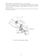

(d) Acceleration and printing control from home position:
By the control of a) and b) of 12), the carriage is moved from left to right (column 1 to column
80).
In this case, reading to recognize the HP signal is done only in the excitation condition memorized
in v) of d). Accordingly the HP signal read timing is every four MTSs.
The print occurs during MTS and thereafter following the MTS where the HIGH of the HP signal is
recognized. The printing occurs during maximum of MTS 816 pulses (DTS2448 pulses).
(e)
Deceleration stop at positions other than home position:
Deceleration control is started from the next MTS (Tm + 1 = T) after the printing of the last dot on the
line (MTS immediately after this if Tm). It is stopped after 18 times of phase switching.
(f)
Acceleration and printing control from positions other than home position:
By the control of a) and b) of 12), the carriage is moved in a chosen direction.
The printing area is the 19th MTS (TN) and thereafter.
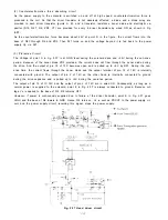
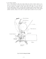
(g) Deceleration and stop at home position
The HP signal is recognized at every MTS during the shift of the carriage from right to left (column 136
to column 1 ), deceleration is started from the next MTS (TM + 1) of the MTS (TM) where the change of
HIGH to LOW of HP signal is recognized, and the CR motor is stopped after 18 phase switches.
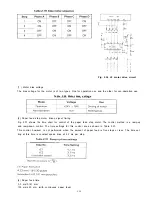
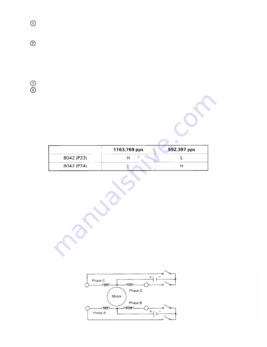
(h) Setting of speed control terminals
In each control mode the terminals of 8042 (P23 and P24) in the Fig. 2.26 must be set as follows:
Table 2.18
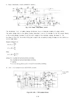
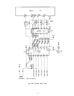
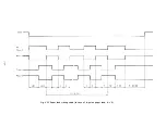
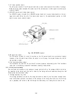
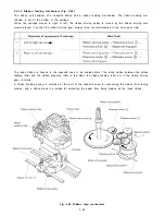
2.4.5 LF motor control circuit (Fig. 2.34)
The control signal of the 4-phase excitation LF motor (Fig. 2.33) is output from CPU 8041 A on the main
circuit board. This signal is sent to IA to ID inputs of the transistor array HA1 3007. With the input at HIGH
Level, the inside transistor turns on, forming a closed circuit of power supply (+24V): LF motor, diode,
HA1 3007, GND, and the current flows through the coil of the LF motor. The LF motor is thus driven with
the voltage-applied phase switched by turning the transistor on and off inside HA1 3007 by the input sig-
nal IA to ID.
The operation mode or the non-operation mode can be selected by the output of P27 of CPU 8041 A.
W ith this output at HIGH, transistor 029 is off and +5V is supplied to LFCOM via resistance R4 and diode
D31, putting the LF motor in the non-operation mode. With the output of P27 at LOW, on the other hand,
transistor Q29 is on and Vp (+24V) is supplied to LFCOM via D30, putting the LF motor in the operation
mode.
Basically, the belt motor is driven by the 2-2 phase excitation system
Fig. 2.33 LF motor circuit
2 - 3 4
Summary of Contents for LQ-1500
Page 1: ...L Q 1 5 0 0 SERVICE MANUAL EPSON a9Printed on Recycled Paper ...
Page 8: ...Table 1 1 3 ...
Page 16: ...Note Direction refers to the direction of signal as viewed from the UXMCL circuit board ...
Page 18: ...2 6 ...
Page 21: ...Note Direction refers to the direction of signal as viewed from the UXDRV circuit board 2 9 ...
Page 39: ...Fig 2 26 CR motor drive circuit 2 2 7 ...
Page 42: ...Table 2 17 Data of decelerate time ...
Page 43: ...Fig 2 29 Deceleration and stop at home position In case of 1163 769 pps ...
Page 48: ...Fig 2 35 Paper feed timing chart In case of N pulse paper feed N 5 ...
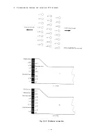
Page 56: ...3 Correspondence between dot wires and FPC terminals Fig 2 45 Printhead connector 2 4 4 ...
Page 64: ...3 3 ...
Page 66: ...3 1 3 3 Handshaking of the parallel interface Fig 3 1 Parallel interface timing 3 5 ...
Page 68: ...3 1 5 Circuit diagram 3 7 ...
Page 69: ...Fig 3 4 Component layout of IUPIF board ...
Page 73: ...D DIP 4 Table 3 10 Setting of DIP 4 3 12 ...
Page 80: ...3 2 4 Block diagram 3 19 ...
Page 81: ...3 2 5 Circuit diagram IURS CIRCUIT BOARD UNIT NO Y49520300000 Fig 3 9 IURS circuit board 3 20 ...
Page 82: ...Fig 3 10 Component layout of IURS board ...
Page 90: ...3 3 5 Block diagram m x 6 IA 3 29 ...
Page 93: ...Fig 3 17 Component layout of IUIE ...
Page 115: ...3 54 ...
Page 116: ...3 55 ...
Page 117: ... Fault of selection and feed 3 56 ...
Page 118: ... Fault of paper guides1 3 57 ...
Page 119: ... Fault of output selector 3 58 ...
Page 120: ... Other faults Paper is fed at an angle 3 59 ...
Page 123: ......
Page 144: ... Mechanical components Model 3660 Y450590100 Maintenance tool 5 3 ...
Page 145: ...5 2 Check out Procedure Repair by Unit Replacement 5 4 ...
Page 146: ...5 5 ...
Page 147: ...5 6 ...
Page 148: ...5 7 ...
Page 149: ... Carriage does not return to home position when power switch is turned on 5 8 ...
Page 150: ... Carriage does not move ...
Page 151: ...5 10 ...
Page 152: ... Control panel indication is faulty Paper feeding motor does not stop 5 11 ...
Page 153: ... Switch on control panel can operate in the on line state 5 12 ...
Page 154: ... Sheet loading does not work properly ...
Page 156: ... Carriage does not move in Self Printing Test 2 5 15 ...
Page 157: ... Paper feeding is not made in Self Printing Test Printing is faulty 5 16 ...
Page 158: ... Operation is abnormal when connected with host computer 5 17 ...
Page 159: ...5 3 Unit Repair Flow Chart UXMCL 5 18 ...
Page 160: ...1 Printing Troubles 5 19 ...
Page 161: ...5 20 ...
Page 162: ... ...
Page 163: ...5 22 ...
Page 164: ...5 23 ...
Page 165: ...2 Carriage Troubles 5 24 ...
Page 166: ...5 25 ...
Page 167: ...5 26 ...
Page 168: ...5 27 ...
Page 169: ...5 28 ...
Page 170: ...3 Paper Feeding Troubles 5 29 ...
Page 171: ...5 30 ...
Page 172: ...5 31 ...
Page 173: ...4 Sheet Loading Problem 5 32 ...
Page 174: ...5 4 Unit Repair Flow Chat t UXDRV 5 33 ...
Page 175: ...1 Printing Troubles 5 34 ...
Page 176: ...5 35 ...
Page 177: ...2 Carriage Troubles 5 36 ...
Page 178: ...3 Paper Feeding Troubles 5 37 ...
Page 179: ...5 38 ...
Page 180: ...4 Sheet Loading Troubles 5 39 ...
Page 181: ...5 5 Unit Repair Flow Chart IUPIF 5 40 ...
Page 182: ...5 41 ...
Page 183: ...5 6 Unit Repair Flow Chart UXPS 5 4 2 ...
Page 184: ... 24 voltage is not output The malfunction of the primary 5 43 ...
Page 186: ...The voltage of 24 is low Excessive voltage is output 5 45 ...
Page 187: ... 5 is abnormal 5 46 ...
Page 188: ...Vx is abnormal 12 is abnormal 5 47 ...
Page 195: ...List of Principal lC s Table 7 1 7 1 ...
Page 209: ...Fig 7 16 Pin configuration 7 15 ...
Page 210: ... 2 Block Diagram 8042 Fig 7 17 Block diagram 7 16 ...
Page 216: ......
Page 229: ...EXPLODED DIAGRAM FOR LQ 1500 12OV VERSION 7 35 ...
Page 230: ......
Page 231: ...7 37 ...
Page 232: ...7 38 ...
Page 233: ......
Page 234: ......
Page 235: ......
Page 236: ......
Page 237: ...UXPS CIRCUIT BOARD UNIT NO Y45020300000 7 43 ...
Page 238: ......
Page 239: ......
Page 240: ......
Page 241: ......


