
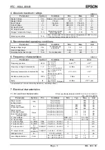
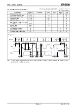
RTC - 8564 JE/NB
Page - 6
MQ - 322 - 04
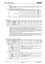
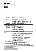
8.2.2. Control register 2
Address
Function
bit 7
bit 6
bit 5
bit 4
bit 3
bit 2
bit 1
bit 0
01 Control
2
0
×
0
TI / TP
AF
TF
AIE
TIE
•
TI/TP ( Interrupt Signal Output Mode Select. Interrupt / Periodic )
If this bit is set to 0, when the timer counts down in the single operation mode and becomes zero, it sets the TF
flag and then stops. If this bit is set to 1, when the timer in the repeat mode becomes zero, it sets the TF flag,
and it furthermore reload the initial value and repeat to count down. As long as the TF flag is not cleared, the
set is maintained.
•
AF ( Alarm Flag )
This is a flag bit which goes into the set state when an alarm occurs.
•
TF ( Timer Flag )
This is a flag bit which goes into the set state when the timer counts down within the specified cycle and
becomes zero.
•
AIE ( Alarm Interrupt Enable )
This bit determines whether to output the alarm flag state to the /INT pin. When it is set to 1, AF=1 then /INT
becomes LOW. When it is set to 0, the information is not output to the /INT pin.
•
TIE ( Timer Interrupt Enable )
This bit determines whether to output the Timer flag state to the /INT pin. When it is set to 1, TF=1 then /INT
becomes LOW. When it is set to 0, the information is not output to the /INT pin.
(Note)
The /INT pin outputs the logical sum of the respective signal of alarm interrupt and timer interrupt. When an
interrupt occurs, the AF/TF flag is read out. Therefore, be sure to check to see which interrupt event has
occurred.When alarm and timer are both prohibited . The /INT pin will not become LOW active. If all hardware
interrupts cannot be used due to system constraints, after the above setup, be sure to use the software to
monitor the interrupt flags for AF and TF.
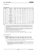
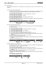
8.2.3. Clock and calendar registers, and VL bit and century bit
Address
Function
bit 7
bit 6
bit 5
bit 4
bit 3
bit 2
bit 1
bit 0
02
Seconds
VL 40 20 10 8 4 2 1
03 Minutes
×
40 20 10 8 4 2 1
04 Hours
×
×
20
10 8 4 2 1
05 Days
×
×
20
10 8 4 2 1
06 Weekdays
×
×
×
×
×
4 2 1
07
Months / Century
C
×
×
10 8 4 2 1
08
Years
80 40 20 10 8 4 2 1
If data and time are set to impossible values, the clock cannot operate correctly. Therefore pay attention when
handling them.
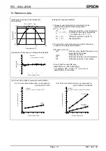
•
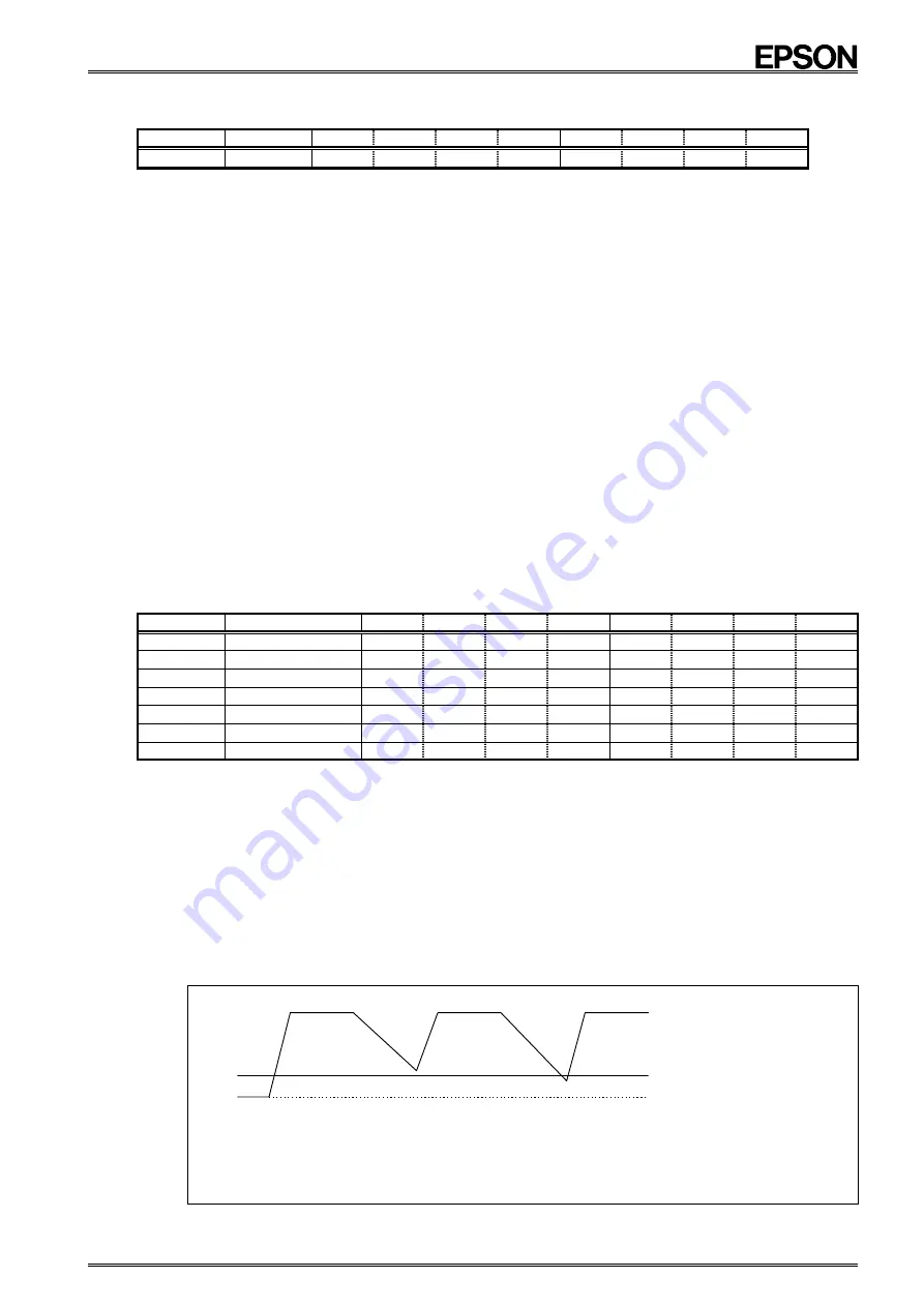
VL ( Voltage Low bit )
This is the bit for detecting low voltage. When the power source's voltage drops below VLOW[V]*, this flag is
set to 1.
After the initial power-on, it is set to 1. If this flag is set to 1 after recovery from the backup state, this means
during the backup the power was low, and all data need to be initialized.
But this bit is intended to detect the situation when V
DD
is decreasing slowly for example under battery
operation.
In other words, chattering doesn't detect it.
However, because this bit is write cleared regardless of the data, before performing a write to this register, be
sure to read out its value.
∗
See the description on DC electrical characteristics.
V
LOW
GND
V
DD
(1) VL=”1”
(2) VL=”0”
(3) VL=”1”
(1) VL="1" as result of initial supply of power
(2) When the power supply is low but voltage not dropping to V
LOW
, VL remains at "0"
with no change
(3) When the power supply is low and voltage dropping below V
LOW
, VL becomes "1".
∗
The value of the VL bit in (2) and (3) need to be zero cleared in (1).
GND=0 V


