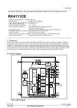
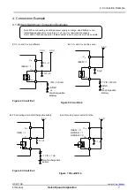
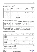
Epson RX4111CE, Applications Manual
The Epson RX4111CE Applications Manual is a comprehensive user guide that covers all the essential features and functions of this cutting-edge product. With step-by-step instructions and detailed illustrations, this manual is available for free download at 88.208.23.73:8080, providing users with easy access to enhance their product experience.
Share
Download


Reviews:
No comments
Related manuals for RX4111CE
100E
Brand: Lathem Pages: 36
Jumbo
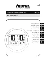
Brand: Hama Pages: 40
180
Brand: QLOCKTWO Pages: 9
Emotion
Brand: Hama Pages: 12
RC300
Brand: Hama Pages: 16
RC300
Brand: Hama Pages: 52

6945
Brand: Dayasa Pages: 12
CWA100
Brand: Hama Pages: 2
00186432
Brand: Hama Pages: 4
Koala
Brand: Hama Pages: 4
PP-245
Brand: Hama Pages: 39

404-1946
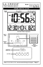
Brand: La Crosse Technology Pages: 2

404-1246
Brand: La Crosse Technology Pages: 2
513-1211
Brand: La Crosse Technology Pages: 4

513-149V2
Brand: La Crosse Technology Pages: 10
W88631
Brand: La Crosse Technology Pages: 2

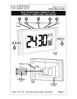
513-1919
Brand: La Crosse Technology Pages: 10
519-1416
Brand: La Crosse Pages: 6


