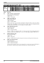
18 UART
214
EPSON
S1C17001 TECHNICAL MANUAL
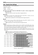
18.4 Transfer Data Settings
Set the following conditions to set the transfer data format.
• Data length: 7 or 8 bits
• Start bit:
Fixed at 1 bit
• Stop bit:
1 or 2 bits
• Parity bit:
Even, odd, no parity
Note: Make sure the UART is halted (when RXEN/UART_CTL register = 0) before changing transfer
data format settings.
∗
RXEN
: UART Enable Bit in the UART Control (UART_CTL) Register (D0/0x4104)
Data length
The data length is selected by CHLN (D4/UART_MOD register). Setting CHLN to 0 (default) sets the data
length to 7 bits. Setting CHLN to 1 sets the data length to 8 bits.
∗
CHLN
: Character Length Select Bit in the UART Mode (UART_MOD) Register (D4/0x4103)
Stop bit
The stop bit length is selected by STPB (D1/UART_MOD register). Setting STPB to 0 (default) sets the stop
bit length to 1 bit. Setting STPB to 1 sets the stop bit length to 2 bits.
∗
STPB
: Stop Bit Select Bit in the UART Mode (UART_MOD) Register (D1/0x4103)
Parity bit
Whether the parity function is enabled or disabled is selected by PREN (D3/UART_MOD register). Setting
PREN to 0 (default) disables the parity function. In this case, no parity bit is added to the transfer data and the
data is not checked for parity when received. Setting PREN to 1 enables the parity function. In this case, a par-
ity bit is added to the transfer data and the data is checked for parity when received.
When the parity function is enabled, the parity mode is selected by PMD (D2/UART_MOD register). Setting
PMD to 0 (default) adds a parity bit and checks for even parity. Setting PMD to 1 adds a parity bit and checks
for odd parity.
∗
PREN
: Parity Enable Bit in the UART Mode (UART_MOD) Register (D3/0x4103)
∗
PMD
: Parity Mode Select Bit in the UART Mode (UART_MOD) Register (D2/0x4103)
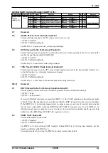
Sampling clock (sclk-1/16)
CHLN = 0, PREN = 0, STPB = 0
CHLN = 0, PREN = 1, STPB = 0
CHLN = 0, PREN = 0, STPB = 1
CHLN = 0, PREN = 1, STPB = 1
CHLN = 1, PREN = 0, STPB = 0
CHLN = 1, PREN = 1, STPB = 0
CHLN = 1, PREN = 0, STPB = 1
CHLN = 1, PREN = 1, STPB = 1
s1: Start bit, s2 & s3: Stop bits, p: Parity bit
s1
D0
D1
D2
D3
D4
D5
D6
s2
s1
D0
D1
D2
D3
D4
D5
D6
p
s2
s1
D0
D1
D2
D3
D4
D5
D6
s2
s3
s1
D0
D1
D2
D3
D4
D5
D6
p
s2
s3
s1
D0
D1
D2
D3
D4
D5
D6
D7
s2
s1
D0
D1
D2
D3
D4
D5
D6
D7
p
s2
s1
D0
D1
D2
D3
D4
D5
D6
D7
s2
s3
s1
D0
D1
D2
D3
D4
D5
D6
D7
p
s2
s3
Figure 18.4.1: Transfer data format
Summary of Contents for S1C17001
Page 1: ...Technical Manual S1C17001 CMOS 16 BIT SINGLE CHIP MICROCONTROLLER ...
Page 33: ...4 POWER SUPPLY VOLTAGE 24 EPSON S1C17001 TECHNICAL MANUAL This page intentionally left blank ...
Page 63: ...6 INITERRUPT CONTROLLER 54 EPSON S1C17001 TECHNICAL MANUAL This page intentionally left blank ...
Page 87: ...8 CLOCK GENERATOR CLG 78 EPSON S1C17001 TECHNICAL MANUAL This page intentionally left blank ...
Page 91: ...9 PRESCALER PSC 82 EPSON S1C17001 TECHNICAL MANUAL This page intentionally left blank ...
Page 133: ...11 16 BIT TIMER T16 124 EPSON S1C17001 TECHNICAL MANUAL This page intentionally left blank ...
Page 211: ...16 STOPWATCH TIMER SWT 202 EPSON S1C17001 TECHNICAL MANUAL This page intentionally left blank ...
Page 219: ...17 WATCHDOG TIMER WDT 210 EPSON S1C17001 TECHNICAL MANUAL This page intentionally left blank ...
Page 241: ...18 UART 232 EPSON S1C17001 TECHNICAL MANUAL This page intentionally left blank ...
Page 277: ...20 I2 C 268 EPSON S1C17001 TECHNICAL MANUAL This page intentionally left blank ...
Page 313: ...25 PACKAGE 304 EPSON S1C17001 TECHNICAL MANUAL This page intentionally left blank ...


