18 UART
224
EPSON
S1C17001 TECHNICAL MANUAL
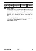
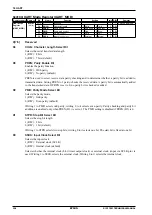
0x4100: UART Status Register (UART_ST)
Register name Address
Bit
Name
Function
Setting
Init. R/W
Remarks
UART Status
Register
(UART_ST)
0x4100
(8 bits)
D7
–
reserved
–
–
–
0 when being read.
D6
FER
Framing error flag
1 Error
0 Normal
0
R/W Reset by writing 1.
D5
PER
Parity error flag
1 Error
0 Normal
0
R/W
D4
OER
Overrun error flag
1 Error
0 Normal
0
R/W
D3
RD2B
Second byte receive flag
1 Ready
0 Empty
0
R
D2
TRBS
Transmit busy flag
1 Busy
0 Idle
0
R
Shift register status
D1
RDRY
Receive data ready flag
1 Ready
0 Empty
0
R
D0
TDBE
Transmit data buffer empty flag
1 Empty
0 Not empty
1
R
D7 Reserved
D6
FER: Framing Error Flag
Indicates whether a framing error has occurred.
1 (R):
Error occurred
0 (R):
No error (default)
1 (W): Reset to 0
0 (W): Disabled
FER is set to 1 when a framing error occurs. Framing errors occur when data is received with the stop
bit set to 0.
FER is reset by writing as 1 or by setting RXEN (D0/UART_CTL register) to 0.
D5
PER: Parity Error Flag
Indicates whether a parity error has occurred.
1 (R):
Error occurred
0 (R):
No error (default)
1 (W): Reset to 0
0 (W): Disabled
PER is set to 1 when a parity error occurs. Parity checking is enabled only when PREN (D3/
UART_MOD register) is set to 1 and is performed when received data is transferred from the shift reg-
ister to the receive data buffer.
PER is reset by writing as 1 or by setting RXEN (D0/UART_CTL register) to 0.
D4
OER: Overrun Error Flag
Indicates whether an overrun error has occurred.
1 (R):
Error occurred
0 (R):
No error (default)
1 (W): Reset to 0
0 (W): Disabled
OER is set to 1 when an overrun error occurs. Overrun errors occur when data is received in the shift
register when the receive data buffer is already full and additional data is sent. The receive data buffer
is not overwritten if this error occurs. The shift register is overwritten as soon as the error occurs.
OER is reset by writing as 1 or by setting RXEN (D0/UART_CTL register) to 0.
D3
RD2B: Second Byte Received Flag
Indicates that the receive data buffer contains two items of received data.
1 (R):
Second byte can be read
0 (R):
Second byte not received (default)
RD2B is set to 1 when the second byte of data is loaded into the receive data buffer and is reset to 0
when the first data is read from the receive data buffer.
Summary of Contents for S1C17001
Page 1: ...Technical Manual S1C17001 CMOS 16 BIT SINGLE CHIP MICROCONTROLLER ...
Page 33: ...4 POWER SUPPLY VOLTAGE 24 EPSON S1C17001 TECHNICAL MANUAL This page intentionally left blank ...
Page 63: ...6 INITERRUPT CONTROLLER 54 EPSON S1C17001 TECHNICAL MANUAL This page intentionally left blank ...
Page 87: ...8 CLOCK GENERATOR CLG 78 EPSON S1C17001 TECHNICAL MANUAL This page intentionally left blank ...
Page 91: ...9 PRESCALER PSC 82 EPSON S1C17001 TECHNICAL MANUAL This page intentionally left blank ...
Page 133: ...11 16 BIT TIMER T16 124 EPSON S1C17001 TECHNICAL MANUAL This page intentionally left blank ...
Page 211: ...16 STOPWATCH TIMER SWT 202 EPSON S1C17001 TECHNICAL MANUAL This page intentionally left blank ...
Page 219: ...17 WATCHDOG TIMER WDT 210 EPSON S1C17001 TECHNICAL MANUAL This page intentionally left blank ...
Page 241: ...18 UART 232 EPSON S1C17001 TECHNICAL MANUAL This page intentionally left blank ...
Page 277: ...20 I2 C 268 EPSON S1C17001 TECHNICAL MANUAL This page intentionally left blank ...
Page 313: ...25 PACKAGE 304 EPSON S1C17001 TECHNICAL MANUAL This page intentionally left blank ...

