19 SPI
238
EPSON
S1C17001 TECHNICAL MANUAL
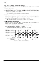
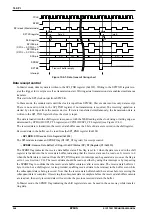
PCLK
SPEN
SPI clock (Master mode)
SPTXD register
Shift register
SPICLK pin
(CPOL = 0, CPHA = 1)
SPICLK pin
(CPOL = 0, CPHA = 0)
SDO pin
SPBSY
SPTBE
Interrupt
A
D7
B
D7
A
D6
A
D0
Write
Write
Transmit buffer empty
Data A
Data B
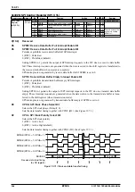
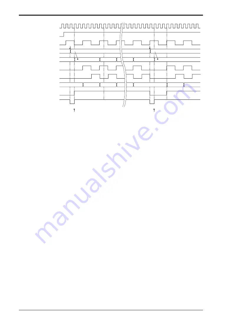
Figure 19.5.1: Data transmit timing chart
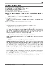
Data receipt control
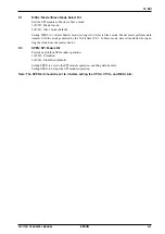
In Master mode, dummy data is written to the SPI_TXD register (0x4322). Writing to the SPI TXD register cre-
ates the trigger for receipt as well as transmission start. Writing actual transmission data enables simultaneous
transfers.
This starts the SPI clock output from SPICLK.
In Slave mode, the module waits until the clock is input from SPICLK. Slave mode involves only data receipt.
There is no need to write to the SPI_TXD register if no transmission is required. The receiving operation is
started by clock input from the master device. If data is transferred simultaneously, the transmission data is
written to the SPI_TXD register before the clock is input.
The data is loaded into the shift register in sequence with the MSB leading at the clock rising or tailing edge, as
determined by CPHA (D3/SPI_CTL register) and CPOL (D2/SPI_CTL register) (see Figure 19.4.1).
The received data is loaded into the receive data buffer once the 8 bits of data are received in the shift register.
Received data in the buffer can be read from the SPI_RXD register (0x4324)
∗
SPI_RXD
: SPI Receive Data Register (0x4324)
The SPI module includes an SPRBF flag (D1/SPI_ST register) for receipt control.
∗
SPRBF
: Receive Data Buffer Full Flag in the SPI Status (SPI_ST) Register (D1/0x4320)
The SPRBF flag indicates the receive data buffer status. This flag is set to 1 when the data received in the shift
register is loaded into the receive data buffer, indicating that the receive data can be read out. It reverts to 0
when the buffer data is read out from the SPI_RXD register. An interrupt can be generated as soon as the flag is
set to 1 (see Section 19.6). The received data should be read out either by using this interrupt or by inspecting
the SPRBF flag to confirm that the receive data buffer contains valid receive data. The receive data buffer is 1
byte in size, but a shift register is also provided, enabling received data to be retained in the buffer even while
the subsequent data is being received. Note that the receive data buffer should be read out before receiving the
subsequent data is complete. If receiving the subsequent data is complete before the receive data buffer contents
are read out, the newly received data will overwrite the previous received data in the buffer.
In Master mode, the SPBSY flag indicating the shift register state can be used in the same way while transfer-
ring data.
Summary of Contents for S1C17001
Page 1: ...Technical Manual S1C17001 CMOS 16 BIT SINGLE CHIP MICROCONTROLLER ...
Page 33: ...4 POWER SUPPLY VOLTAGE 24 EPSON S1C17001 TECHNICAL MANUAL This page intentionally left blank ...
Page 63: ...6 INITERRUPT CONTROLLER 54 EPSON S1C17001 TECHNICAL MANUAL This page intentionally left blank ...
Page 87: ...8 CLOCK GENERATOR CLG 78 EPSON S1C17001 TECHNICAL MANUAL This page intentionally left blank ...
Page 91: ...9 PRESCALER PSC 82 EPSON S1C17001 TECHNICAL MANUAL This page intentionally left blank ...
Page 133: ...11 16 BIT TIMER T16 124 EPSON S1C17001 TECHNICAL MANUAL This page intentionally left blank ...
Page 211: ...16 STOPWATCH TIMER SWT 202 EPSON S1C17001 TECHNICAL MANUAL This page intentionally left blank ...
Page 219: ...17 WATCHDOG TIMER WDT 210 EPSON S1C17001 TECHNICAL MANUAL This page intentionally left blank ...
Page 241: ...18 UART 232 EPSON S1C17001 TECHNICAL MANUAL This page intentionally left blank ...
Page 277: ...20 I2 C 268 EPSON S1C17001 TECHNICAL MANUAL This page intentionally left blank ...
Page 313: ...25 PACKAGE 304 EPSON S1C17001 TECHNICAL MANUAL This page intentionally left blank ...


