20 I
2
C
S1C17001 TECHNICAL MANUAL
EPSON
265
0x4344: I
2
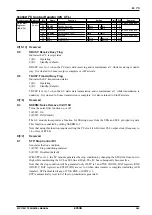
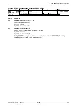
C Data Register (I2C_DAT)
Register name Address
Bit
Name
Function
Setting
Init. R/W
Remarks
I
2
C Data
Register
(I2C_DAT)
0x4344
(16 bits)
D15–12
–
reserved
–
–
–
0 when being read.
D11
RBRDY
Receive buffer ready
1 Ready
0 Empty
0
R
D10
RXE
Receive execution
1 Receive
0 Ignored
0
R/W
D9
TXE
Transmit execution
1 Transmit
0 Ignored
0
R/W
D8
RTACK
Receive/transmit ACK
1 Error
0 ACK
0
R/W
D7–0
RTDT[7:0]
Receive/transmit data
RTDT7 = MSB
RTDT0 = LSB
0x0 to 0xff
0x0
R/W
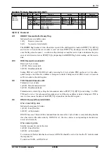
D[15:12] Reserved
D11
RBRDY: Receive Buffer Ready Flag
Indicates the receive buffer status.
1 (R):
Receive data exists
0 (R):
No receive data (default)
The RBRDY flag becomes 1 when the data received in the shift register is loaded to RTDT[7:0] (D[7:0])
and reverts to 0 when the receive data is read out from RTDT[7:0]. Interrupts can also be generated
once the flag value becomes 1, so either use this interrupt or read the receive data to determine the pres-
ence of valid receive data in RTDT[7:0] by inspecting the RBRDY flag before reading out the receive
data.
D10
RXE: Receive Execution Bit
Receives 1 byte of data.
1 (R/W): Data receipt start
0 (R/W): Disabled (default)
Setting RXE to 1 and TXE (D9) to 0 starts receiving for 1 byte of data. RXE can be set to 1 for subse-
quent receipt, even if the slave address is being sent or data is being received. RXE is reset to 0 as soon
as D6 is loaded to the shift register.
D9
TXE: Transmit Execution Bit
Transmits 1 byte of data.
1 (R/W): Data transmission start
0 (R/W): Disabled (default)
Transmission is started by setting the transmission data to RTDT[7:0] (D[7:0]) and writing 1 to TXE.
TXE can be set to 1 for subsequent transmission, even if the slave address or data is being sent. TXE is
reset to 0 as soon as the data set in RTDT[7:0] is transferred to the shift register.
D8
RTACK: Receive/Transmit ACK Bit
When transmitting data
Indicates the response bit status.
1 (R/W): Error (NACK)
0 (R/W): ACK (default)
RTACK becomes 0 when ACK is returned from the slave after 1 byte of data is sent, indicating that the
slave has received the data correctly. If RTACK is 1, the slave device is not operating or the data was
not received correctly.
When receiving data
Sets the response bit sent to the slave.
1 (R/W): Error (NACK)
0 (R/W): ACK (default)
To return an ACK after data has been received, RTACK should be set to 0 before the I
2
C module sends
the response bit.
To return an NACK, set RTACK to 1.
Summary of Contents for S1C17001
Page 1: ...Technical Manual S1C17001 CMOS 16 BIT SINGLE CHIP MICROCONTROLLER ...
Page 33: ...4 POWER SUPPLY VOLTAGE 24 EPSON S1C17001 TECHNICAL MANUAL This page intentionally left blank ...
Page 63: ...6 INITERRUPT CONTROLLER 54 EPSON S1C17001 TECHNICAL MANUAL This page intentionally left blank ...
Page 87: ...8 CLOCK GENERATOR CLG 78 EPSON S1C17001 TECHNICAL MANUAL This page intentionally left blank ...
Page 91: ...9 PRESCALER PSC 82 EPSON S1C17001 TECHNICAL MANUAL This page intentionally left blank ...
Page 133: ...11 16 BIT TIMER T16 124 EPSON S1C17001 TECHNICAL MANUAL This page intentionally left blank ...
Page 211: ...16 STOPWATCH TIMER SWT 202 EPSON S1C17001 TECHNICAL MANUAL This page intentionally left blank ...
Page 219: ...17 WATCHDOG TIMER WDT 210 EPSON S1C17001 TECHNICAL MANUAL This page intentionally left blank ...
Page 241: ...18 UART 232 EPSON S1C17001 TECHNICAL MANUAL This page intentionally left blank ...
Page 277: ...20 I2 C 268 EPSON S1C17001 TECHNICAL MANUAL This page intentionally left blank ...
Page 313: ...25 PACKAGE 304 EPSON S1C17001 TECHNICAL MANUAL This page intentionally left blank ...

