Page 104
Epson Research and Development
Vancouver Design Center
S1D13504
Hardware Functional Specification
X19A-A-002-19
Issue Date: 01/11/06
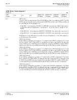
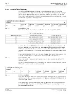
bit 3
GPIO11 Pin IO Configuration
When this bit = 1, GPIO11 is configured as an output. When this bit = 0 (default), GPIO11 is con-
figured as an input. Note the MD8 pin must be high at the rising edge of RESET# to enable
GPIO11, otherwise the VRTC pin is controlled automatically and this bit will have no effect on
hardware.
bit 2
GPIO10 Pin IO Configuration
When this bit = 1, GPIO10 is configured as an output. When this bit = 0 (default), GPIO10 is con-
figured as an input. Note the MD8 pin must be high at the rising edge of RESET# to enable
GPIO10, otherwise the HRTC pin is controlled automatically and this bit will have no effect on
hardware.
bit 1
GPIO9 Pin IO Configuration
When this bit = 1, GPIO9 is configured as an output. When this bit = 0 (default), GPIO9 is config-
ured as an input.
Note
GPIO9 and GPIO8 must always be set to the same function (both to input or both to output).
The MD8 pin must be high at the rising edge of RESET# to enable GPIO9, otherwise the DACRS1
pin is controlled automatically and this bit will have no effect on hardware.
bit 0
GPIO8 Pin IO Configuration
When this bit = 1, GPIO8 is configured as an output. When this bit = 0 (default), GPIO8 is config-
ured as an input.
Note
GPIO8 and GPIO9 must always be set to the same function (both to input or both to output).
The MD8 pin must be high at the rising edge of RESET# to enable GPIO8, otherwise the DACRS0
pin is controlled automatically and this bit will have no effect on hardware.
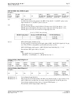
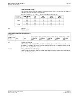
GPIO Configuration Register 1
REG[1Fh]
RW
n/a
n/a
n/a
n/a
GPIO11 Pin
IO Config.
GPIO10 Pin
IO Config.
GPIO9 Pin
IO Config.
GPIO8 Pin
IO Config.

