Epson Research and Development
Page 59
Vancouver Design Center
Programming Notes and Examples
S1D13504
Issue Date: 01/02/01
X19A-G-002-07
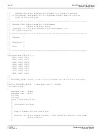
/*
** Register 16-17: Memory Address Offset - this address represents the
** starting WORD. At 8BPP our 320 pixel width is 160
** WORDS
*/
*(pRegs + 0x16) = 0xA0; /* 1010 0000 */
*(pRegs + 0x17) = 0x00; /* 0000 0000 */
/*
** Register 18: Pixel Panning -
*/
*(pRegs + 0x18) = 0x00; /* 0000 0000 */
/*
** Register 19: Clock Configuration - In this case we must divide
** MCLK by 4 to arrive at the best frequency to set
** our desired panel frame rate.
*/
*(pRegs + 0x19) = 0x03; /* 0000 0011 */
/*
** Register 1A: Power Save Configuration - enable LCD power, CBR refresh,
** not suspended.
*/
*(pRegs + 0x1A) = 0x00; /* 0000 0000 */
/*
** Register 1C-1D: MD Configuration Readback - don't write anything to
** these registers.
*/
/*
** Register 1E-1F: General I/O Pins Configuration - these values
** may need to be changed according to your system
*/
*(pRegs + 0x1E) = 0x00; /* 0000 0000 */
*(pRegs + 0x1F) = 0x00; /* 0000 0000 */
/*
** Register 20-21: General I/O Pins Control - these values
** may need to be changed according to your system
*/
*(pRegs + 0x20) = 0x00; /* 0000 0000 */
*(pRegs + 0x21) = 0x00; /* 0000 0000 */
/*
** Registers 24-27: LUT control.
** For this example do a typical 8BPP LUT setup.
** In 8BPP mode only the first 8 red, first 8 green
** and first 4 blue values are used.
**
** Setup the pointer to the LUT data and reset the LUT index register.
** Then, loop writing each of the RGB LUT data elements.
*/
pLUT = LUT8;
*(pRegs + 0x24) = 0;

