Epson Research and Development
Page 23
Vancouver Design Center
Hardware Functional Specification
S1D13504
Issue Date: 01/11/06
X19A-A-002-19
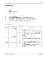
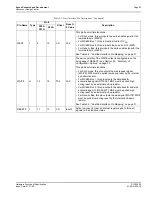
WE0#
I
8
10
CS
Hi-Z
This pin has multiple functions.
• For SH-3 mode, this pin inputs the write enable signal for the
lower data byte (WE0#).
• For MC68K Bus 1, this pin must be tied to IO V
DD.
• For MC68K Bus 2, this pin inputs the bus size bit 0 (SIZ0).
• For Generic Bus, this pin inputs the write enable signal for the
lower data byte (WE0#).
See Table 5-9: “Host Bus Interface Pin Mapping,” on page 31.
WAIT#
O
13
15
TS2
Hi-Z
The active polarity of the WAIT# output is configurable on the
rising edge of RESET# - see Section 5.5,
“Summary of
Configuration Options” on page 30.
This pin has multiple functions.
• For SH-3 mode, this pin outputs the wait request signal
(WAIT#); MD5 must be pulled low during reset by the internal
pull-down resistor.
• For MC68K Bus 1, this pin outputs the data transfer
acknowledge signal (DTACK#); MD5 must be pulled high
during reset by an external pull-up resistor.
• For MC68K Bus 2, this pin outputs the data transfer and size
acknowledge bit 1 (DSACK1#); MD5 must be pulled high
during reset by an external pull-up resistor.
• For Generic Bus, this pin outputs the wait signal (WAIT#); MD5
must be pulled low during reset by the internal pull-down
resistor.
See Table 5-9: “Host Bus Interface Pin Mapping,” on page 31.
RESET#
I
11
13
CS
Input 0
Active low input to clear all internal registers and to force all
signals to their inactive states.
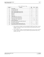
Table 5-1: Host Interface Pin Descriptions (Continued)
Pin Name
Type
Pin #
Driver
Reset =
0 Value
Description
F00A
F01A
F02A

