Epson Research and Development
Page 25
Vancouver Design Center
Hardware Functional Specification
S1D13504
Issue Date: 01/11/06
X19A-A-002-19
1
When configured as IO pins.
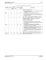
MA[8:0]
O
43, 41,
39, 37,
35, 34,
36, 38,
40
46, 44,
42, 40,
41, 43,
45, 47,
49
CO1
Output 0
Multiplexed memory address.
MA9
IO
45
51
C/TS1
Hi-Z /
Output 0
1
This pin has multiple functions.
• For 2M byte DRAM, this is memory address bit 9 (MA9).
• For asymmetrical 512K byte DRAM, this is memory address
bit 9 (MA9).
• For symmetrical 512K byte DRAM, this pin can be used as
general purpose IO (GPIO3).
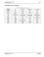
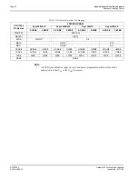
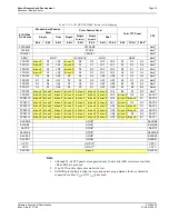
See Table 5-10: “Memory Interface Pin Mapping,” on page 32
for summary.
MA10
IO
42
48
C/TS1
Hi-Z /
Output 0
1
This pin has multiple functions.
• For asymmetrical 2M byte DRAM, this is memory address bit
10 (MA10).
• For symmetrical 2M byte DRAM and all 512K byte DRAM,
this pin can be used as general purpose IO (GPIO1).
See Table 5-10: “Memory Interface Pin Mapping,” on page 32
for summary.
MA11
IO
44
50
C/TS1
Hi-Z /
Output 0
1
This pin has multiple functions.
• For asymmetrical 2M byte DRAM, this is memory address bit
11 (MA11).
• For symmetrical 2M byte DRAM and all 512K byte DRAM,
this pin can be used as general purpose IO (GPIO2).
See Table 5-10: “Memory Interface Pin Mapping,” on page 32
for summary.
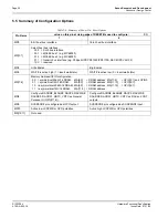
Table 5-2: Memory Interface Pin Descriptions (Continued)
Pin Name Type
Pin #
Driver
Reset = 0
Value
Description
F00A
F01A
F02A

