Epson Research and Development
Page 15
Vancouver Design Center
S5U13504B00C Rev. 2.0 PCI Evaluation Board User Manual
S1D13504
Issue Date: 2002/12/02
X19A-G-014-01
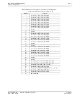
4.2.1 CPU Interface Pin Mapping
The functions of the S1D13504 host interface pins are mapped to each host bus interface
according to the following table.
Note
1
A0 for these busses is not used internally by the S1D13504.
Table 4-1: CPU Interface Pin Mapping
S1D13504
Pin Names
Generic
Hitachi SH-3
Motorola
MC68K Bus 1
Motorola
MC68K Bus 2
AB20
A20
A20
A20
A20
AB19
A19
A19
A19
A19
AB18
A18
A18
A18
A18
AB17
A17
A17
A17
A17
AB[16:13]
A[16:13]
A[16:13]
A[16:13]
A[16:13]
AB[12:1]
A[12:1]
A[12:1]
A[12:1]
A[12:1]
AB0
A0
1
A0
1
LDS#
A0
DB[15:8]
D[15:0]
D[15:8]
D[15:8]
D[31:24]
DB[7:0]
D[7:0]
D[7:0]
D[7:0]
D[23:16]
WE1#
WE1#
WE1#
UDS#
DS#
M/R#
External Decode
CS#
External Decode
BUSCLK
BCLK
CKIO
CLK
CLK
BS#
Connected to IOV
DD
BS#
AS#
AS#
RD/WR#
RD1#
RD/WR#
R/W#
R/W#
RD#
RD0#
RD#
Connected to IOV
DD
SIZ1
WE0#
WE0#
WE0#
Connected to IOV
DD
SIZ0
WAIT#
WAIT#
RDY#
/WAIT#
DTACK#
DSACK1#
RESET#
RESET#
RESET#
RESET#
RESET#

