Page 14
Epson Research and Development
Vancouver Design Center
S1D13504
Interfacing to the Motorola MC68328 "Dragonball" Microprocessor
X19A-G-013-03
Issue Date: 01/10/26
4.3 MC68328 Chip Select Configuration
In the example interface, chip select CSB3 is used to control the S1D13504. A 4M byte
address space is used. The S1D13504 control registers are mapped into the bottom half of
this address block, while the display buffer is mapped into the top half. The chip select
should have its RO (Read Only) bit set to 0, and the WAIT field (Wait states) should be set
to 111 to allow the S1D13504 to terminate bus cycles externally.
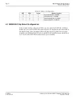
Table 4-3: Memory Configuration
MD7
MD6
Option
Memory Selection
0
0
1
Symmetrical 256K x 16 DRAM
0
1
2
Symmetrical 1M x 16 DRAM
1
0
3
Asymmetrical 256K x 16 DRAM
1
1
4
Asymmetrical 1M x 16 DRAM


