Epson Research and Development
Page 15
Vancouver Design Center
Interfacing to the Motorola MCF5307 "Coldfire" Microprocessor
S1D13504
Issue Date: 01/02/02
X19A-G-011-07
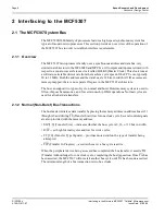
4.3 Memory/Register Mapping
The S1D13504 is a memory mapped device requiring a 2M byte address space for the
display buffer and a few more locations for the internal registers. Chip selects 0 and 1 have
programmable block sizes from 64K bytes through 2G bytes, however these chip selects
would normally be needed to control system RAM and ROM. Two of the IO chip selects
(CS2 through CS7) are required to address the entire address space of the S1D13504, since
these chip selects have a fixed 2M byte block size.
4.4 MCF5307 Chip Select Configuration
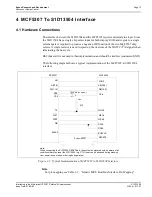
In the example interface, chip selects 4 and 5 are used to control the S1D13504. CS4 selects
a 2M byte address space for the S1D13504 control registers, while CS5 selects the 2M byte
display buffer. The CSBAR register should be set to the upper 8 bits of the desired base
address.
The following options should be selected in the chip select mask registers (CSMR4/5):
• WP = 0 – disable write protect
• AM = 0 - enable alternate bus master access to the S1D13504
• C/I = 1 - disable CPU space access to the S1D13504
• SC = 1 - disable Supervisor Code space access to the S1D13504
• SD = 0 - enable Supervisor Data space access to the S1D13504
• UC = 1 - disable User Code space access to the S1D13504
• UD = 0 - enable User Data space access to the S1D13504
• V = 1 - global enable (“Valid”) for the chip select
The following options should be selected in the chip select control registers (CSCR4/5):
• WS0-3 = 0 - no internal wait state setting
• AA = 0 - no automatic acknowledgment
• PS (1:0) = 1:0 – memory port size is 16 bits
• BEM = 0 – Byte enable/write enable active on writes only
• BSTR = 0 – disable burst reads
• BSTW = 0 – disable burst writes

