Epson Research and Development
Page 17
Vancouver Design Center
Interfacing to the Toshiba MIPS TX3912 Processor
S1D13504
Issue Date: 01/10/26
X19A-G-012-05
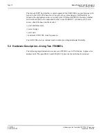
Figure 5-2: S1D13504 to TX3912 Connection using Two IT8368E
Note
For pin mapping see Table 3-1:, “Generic MPU Host Bus Interface Pin Mapping”.
IT8368E
S1D13504
A[12:0]
AB[12:0]
D[31:24]
DB[7:0]
LHA23/MFIO10
WE1#
WE0#
RD1#
RD0#
CS#
LHA22/MFIO9
LHA21/MFIO8
LHA20/MFIO7
LHA19/MFIO6
WAIT#
CARDxWAIT*
M/R#
RESET#
AB[20:13]
LHA23
TX3912
D[23:16]
DB[15:8]
DCLKOUT
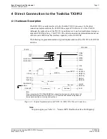
Notes: The Chip Select Logic shown above is necessary to guarantee the timing parameter t1
of the Generic MPU Host Bus Interface Asynchronous Timing (for details refer to the
S1D13504 Hardware
Functional Specification, document number X19A-A-002-xx).
IT8368E
Chip Select
Logic
LHA[20:13],
System RESET
ENDIAN
BUSCLK
Oscillator
...or...
pull-up
V
DD
BS#
IO V
DD
Clock divider
CLKI
See text
LHA23
When connecting the S1D13504 RESET# pin, the system designer should be aware of all conditions
that amy reset the S1D13504 (e.g. CPU reset can be asserted during wake-up from power-down modes,
or during debug states).

