background image

Page 60

Epson Research and Development

Vancouver Design Center

S1D13704

Programming Notes and Examples

X26A-G-002-03

Issue Date: 01/02/12

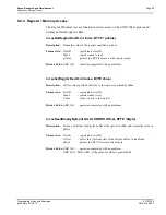
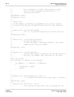
int seGetLut(int DevID, BYTE *pLUT, int Count)

Description:  This routine reads one or more LUT entries and puts the result in the byte array 

pointed to by pLUT.

A Look-Up Table entry consists of three bytes, one each for Red, Green, and Blue. 
The color information is stored in the four least significant bits of each byte.

Parameters: DevID

registered 

device 

ID

pLUT

- pointer to an array of BYTE lut[16][3]
- pLUT must point to enough memory to hold 'Countx 3 bytes of data.

Count

- the number of LUT elements to read.

Return Value: ERR_OK - operation completed with no problems

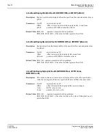
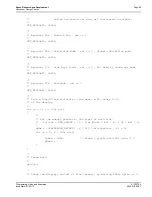
int seSetLutEntry(int DevID, int Index, BYTE *pEntry)

Description:  This routine writes one LUT entry. Unlike seSetLut, the LUT entry indicated by 

'Index' can be any value from 0 to 15.

A Look-Up Table entry consists of three bytes, one each for Red, Green, and Blue. 
The color information is stored in the four least significant bits of each byte.

Parameters: DevID

registered 

device 

ID

Index

- index to LUT entry (0 to 15)

pLUT

- pointer to an array of three bytes.

Return Value: ERR_OK - operation completed with no problems

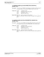
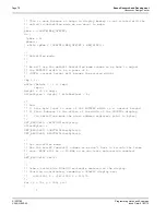
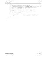
int seGetLutEntry(int DevID, int index, BYTE *pEntry)

Description:  This routine reads one LUT entry from any index.

A Look-Up Table entry consists of three bytes, one each for Red, Green, and Blue. 
The color information is stored in the four least significant bits of each byte.

Parameters: DevID

registered 

device 

ID

Index

- index to LUT entry (0 to 15)

pEntry

- pointer to an array of three bytes

Return Value: ERR_OK - operation completed with no problems

*

Summary of Contents for S1D13704

Page 1: ...his document but only for your own use in evaluating Seiko Epson EPSON products You may not modify the document Epson Research and Development Inc disclaims any representation that the contents of this document are accurate or current The Programs Technologies described in this document may contain material protected under U S and or International Patent laws EPSON is a registered trademark of Sei...

Page 2: ...Page 2 Epson Research and Development Vancouver Design Center S1D13704 TECHNICAL MANUAL X26A Q 001 04 Issue Date 01 02 12 THIS PAGE LEFT BLANK ...

Page 3: ...tain these programs contact Application Engineering Support Application Engineering Support Engineering and Sales Support is provided by Japan Seiko Epson Corporation Electronic Devices Marketing Division 421 8 Hino Hino shi Tokyo 191 8501 Japan Tel 042 587 5812 Fax 042 587 5564 http www epson co jp Hong Kong Epson Hong Kong Ltd 20 F Harbour Centre 25 Harbour Road Wanchai Hong Kong Tel 2585 4600 F...

Page 4: ...Page 4 Epson Research and Development Vancouver Design Center S1D13704 TECHNICAL MANUAL X26A Q 001 04 Issue Date 01 02 12 THIS PAGE LEFT BLANK ...

Page 5: ...4VIRT Display Utility 13704PLAY Diagnostic Utility 13704BMP Demonstration Program 13704PWR Power Save Utility DRIVERS S1D13704 Windows CE Display Drivers EVALUATION S5U13704B00C Rev 1 ISA Bus Evaluation Board User Manual APPLICATION NOTES Interfacing to the Toshiba MIPS TX3912 Processor Power Consumption Interfacing to the Motorola MC68328 Microprocessor Interfacing to the NEC VR4102 Microprocesso...

Page 6: ...Page 6 Epson Research and Development Vancouver Design Center S1D13704 TECHNICAL MANUAL X26A Q 001 04 Issue Date 01 02 12 THIS PAGE LEFT BLANK ...

Page 7: ...terface 4 8 bit color LCD interface Single panel single drive passive displays Dual panel dual drive passive displays Active Matrix TFT TFD interface Register level suport for EL panels Example resolutions 640x480 at a color depth of 1 bpp 640x240 at a color depth of 2 bpp 320x240 at a color depth of 4 bpp 240x160 at a color depth of 8 bpp Power Down Modes Hardware and software Suspend modes LCD p...

Page 8: ...ei Taiwan R O C Tel 02 2717 7360 Fax 02 2712 9164 Singapore Epson Singapore Pte Ltd No 1 Temasek Avenue 36 00 Millenia Tower Singapore 039192 Tel 337 7911 Fax 334 2716 Europe Epson Europe Electronics GmbH Riesstrasse 15 80992 Munich Germany Tel 089 14005 0 Fax 089 14005 110 North America Epson Electronics America Inc 150 River Oaks Parkway San Jose CA 95134 USA Tel 408 922 0200 Fax 408 922 0238 ht...

Page 9: ...ument but only for your own use in evaluating Seiko Epson EPSON products You may not modify the document Epson Research and Development Inc disclaims any representation that the contents of this document are accurate or current The Programs Technologies described in this document may contain material protected under U S and or International Patent laws EPSON is a registered trademark of Seiko Epso...

Page 10: ...Page 2 Epson Research and Development Vancouver Design Center S1D13704 Hardware Functional Specification X26A A 001 04 Issue Date 01 02 08 THIS PAGE LEFT BLANK ...

Page 11: ...am 15 4 1 Functional Block Descriptions 15 4 1 1 Host Interface 15 4 1 2 Memory Controller 15 4 1 3 Sequence Controller 15 4 1 4 Look Up Table 16 4 1 5 LCD Interface 16 4 1 6 Power Save 16 5 Pins 17 5 1 Pinout Diagram 17 5 2 Pin Description 18 5 2 1 Host Interface 18 5 2 2 LCD Interface 20 5 2 3 Clock Input 21 5 2 4 Miscellaneous 21 5 2 5 Power Supply 21 5 3 Summary of Configuration Options 22 5 4...

Page 12: ...ng 47 7 3 9 Dual Color 8 Bit Panel Timing 49 7 3 10 9 12 Bit TFT D TFD Panel Timing 51 8 Registers 54 8 1 Register Mapping 54 8 2 Register Descriptions 54 9 Frame Rate Calculation 70 10 Display Data Formats 71 11 Look Up Table Architecture 72 11 1 Gray Shade Display Modes 72 11 2 Color Display Modes 75 12 SwivelView 79 12 1 Default SwivelView Mode 79 12 1 1 How to Set Up Default SwivelView Mode 80...

Page 13: ... Timing 33 Table 7 7 Clock Input Requirements 34 Table 7 8 Power Down Up Timing 36 Table 8 1 Panel Data Format 55 Table 8 2 Gray Shade Color Mode Selection 56 Table 8 3 High Performance Selection 56 Table 8 4 Inverse Video Mode Select Options 57 Table 8 5 Hardware Power Save GPIO0 Operation 58 Table 8 6 Software Power Save Mode Selection 58 Table 8 7 Look Up Table Access 65 Table 8 8 Selection of ...

Page 14: ...Page 6 Epson Research and Development Vancouver Design Center S1D13704 Hardware Functional Specification X26A A 001 04 Issue Date 01 02 08 THIS PAGE LEFT BLANK ...

Page 15: ...ingle Monochrome 4 Bit Panel Timing 37 Figure 7 11 Single Monochrome 4 Bit Panel A C Timing 38 Figure 7 12 Single Monochrome 8 Bit Panel Timing 39 Figure 7 13 Single Monochrome 8 Bit Panel A C Timing 40 Figure 7 14 Single Color 4 Bit Panel Timing 41 Figure 7 15 Single Color 4 Bit Panel A C Timing 42 Figure 7 16 Single Color 8 Bit Panel Timing Format 1 43 Figure 7 17 Single Color 8 Bit Panel A C Ti...

Page 16: ...el Color Look Up Table Architecture 75 Figure 11 6 4 Level Color Mode Look Up Table Architecture 76 Figure 11 7 16 Level Color Mode Look Up Table Architecture 77 Figure 11 8 256 Level Color Mode Look Up Table Architecture 78 Figure 12 1 Relationship Between The Screen Image and the Image Refreshed by S1D13704 79 Figure 12 2 Relationship Between The Screen Image and the Image Refreshed by S1D13704 ...

Page 17: ...ppreciate your comments on our documentation Please contact us via email at techpubs erd epson com 1 2 Overview Description The S1D13704 is a color monochrome LCD graphics controller with an embedded 40K Byte SRAM display buffer The high integration of the S1D13704 provides a low cost low power single chip solution to meet the requirements of embedded markets such as Office Automation equipment Mo...

Page 18: ...ers Single level CPU write buffer Registers are mapped into upper 32 bytes of 64K byte address space The complete 40K byte frame buffer is directly and contiguously available through the 16 bit address bus 2 3 Display Support 4 8 bit monochrome LCD interface 4 8 bit color LCD interface Single panel single drive passive displays Dual panel dual drive passive displays Active Matrix TFT D TFD interfa...

Page 19: ...display for all landscape panel modes allows two different images to be simultaneously displayed Virtual display support displays images larger than the panel size through the use of panning 2 5 Clock Source Maximum operating clock CLK frequency of 25MHz Operating clock CLK is derived from CLKI input CLK CLKI or CLK CLKI 2 Pixel Clock PCLK and Memory Clock MCLK are derived from CLK 2 6 Miscellaneo...

Page 20: ...3704 FPFRAME FPSHIFT FPLINE DRDY FPDAT 7 0 CLKI Oscillator FPFRAME FPSHIFT FPLINE MOD D 7 0 8 bit LCD Display SH 4 BUS RESET WE0 D 15 0 BS RD WR RD RDY A 15 0 CKIO WE0 RD WR AB 15 0 DB 15 0 WE1 BS RD CS BCLK WAIT RESET CSn WE1 LCDPWR S1D13704 FPFRAME FPSHIFT FPLINE DRDY FPDAT 3 0 CLKI Oscillator FPFRAME FPSHIFT FPLINE MOD D 3 0 4 bit LCD Display SH 3 BUS RESET WE0 D 15 0 BS RD WR RD WAIT A 15 0 CK...

Page 21: ...CLKI Oscillator FPFRAME FPSHIFT FPLINE MOD D 3 0 4 bit LCD Display MC68000 BUS RESET LDS D 15 0 AS R W DTACK A 15 1 CLK AB0 RD WR AB 15 1 DB 15 0 WE1 BS CS BCLK WAIT RESET A 23 16 FC0 FC1 FC2 Decoder UDS LCDPWR S1D13704 FPFRAME FPSHIFT FPLINE DRDY FPDAT 7 0 CLKI Oscillator FPFRAME FPSHIFT FPLINE MOD D 7 0 8 bit LCD Display MC68030 BUS RESET SIZ0 D 31 16 AS R W SIZ1 DSACK1 A 15 0 CLK WE0 RD WR AB 1...

Page 22: ...FPLINE DRDY FPDAT 11 0 CLKI Oscillator FPFRAME FPSHIFT FPLINE DRDY D 11 0 12 bit TFT Display GENERIC 1 BUS RESET D 15 0 RD0 WAIT A 15 0 BCLK RD WR AB 15 0 DB 15 0 WE1 RD CS BCLK WAIT RESET CSn WE1 LCDPWR WE0 WE0 BS RD1 S1D13704 FPFRAME FPSHIFT FPLINE DRDY FPDAT 8 0 CLKI Oscillator FPFRAME FPSHIFT FPLINE DRDY D 8 0 9 bit TFT Display ISA BUS RESET SD 15 0 SMEMR IOCHRDY SA 15 0 BCLK AB 15 0 DB 15 0 W...

Page 23: ...registers 4 1 2 Memory Controller The Memory Controller arbitrates between CPU accesses and display refresh accesses It also generates the necessary signals to control the SRAM frame buffer 4 1 3 Sequence Controller The Sequence Controller controls data flow from the Memory Controller through the Look Up Table and to the LCD Interface It also generates memory addresses for display refresh accesses...

Page 24: ...three 16x4 Look Up Tables or palettes one for each primary color In monochrome mode only one of these Look Up Tables is used 4 1 5 LCD Interface The LCD Interface performs frame rate modulation for passive LCD panels It also generates the correct data format and timing control signals for various LCD and TFT D TFD panels 4 1 6 Power Save Power Save contains the power save mode circuitry ...

Page 25: ...80 79 78 77 76 75 74 73 72 71 70 69 68 67 66 65 64 63 62 61 21 22 23 24 25 26 34 35 36 37 38 39 27 28 29 30 31 32 33 40 S1D13704 IOVDD DB6 DB5 DB4 DB3 DB2 DB0 DB1 COREVDD DB8 DRDY FPDAT7 COREVDD GPIO0 AB3 VSS AB4 AB5 AB6 AB11 AB14 FPDAT11 FPDAT10 FPDAT9 VSS FPSHIFT IOVDD FPDAT5 FPDAT4 FPDAT3 FPDAT2 FPDAT1 FPDAT0 FPLINE FPFRAME VSS CNF2 DB12 DB9 DB10 DB11 DB13 DB14 DB15 WAIT VSS RD WR WE1 WE0 RD BS...

Page 26: ... Pin Cell RESET State Description AB0 I 70 CS Input This pin has multiple functions For SH 3 SH 4 mode this pin inputs system address bit 0 A0 For MC68K 1 this pin inputs the lower data strobe LDS For MC68K 2 this pin inputs system address bit 0 A0 For Generic 1 this pin inputs system address bit 0 A0 For Generic 2 this pin inputs system address bit 0 A0 See Host Bus Interface Pin Mapping for summ...

Page 27: ... data byte WE1 For Generic 2 this pin inputs the byte enable signal for the high data byte BHE See Host Bus Interface Pin Mapping for summary CS I 74 C Input This pin inputs the chip select signal BCLK I 71 C Input This pin inputs the system bus clock BS I 75 CS Input This pin has multiple functions For SH 3 SH 4 mode this pin inputs the bus start signal BS For MC68K 1 this pin inputs the address ...

Page 28: ...data transfer and size acknowledge bit 1 DSACK1 For Generic 1 this pin outputs the wait signal WAIT For Generic 2 this pin outputs the wait signal WAIT See Host Bus Interface Pin Mapping for summary RESET I 73 CS 0 Active low input to set all internal registers to the default state and to force all signals to their inactive states Pin Name Type Pin Cell RESET State Description FPDAT 7 0 O 30 31 32...

Page 29: ...ary Pin Name Type Pin Driver Description CLKI I 51 C Input Clock Pin Name Type Pin Cell RESET State Description CNF 4 0 I 45 46 47 48 49 C As set by hardware These inputs are used to configure the S1D13704 see Summary of Configuration Options Must be connected directly to IO VDD or VSS GPIO0 I O I 22 CS TS1 Input This pin has multiple functions see REG 03h bit 2 General Purpose Input Output pin Ha...

Page 30: ... bit 1 0 0 X reserved 1 0 1 X MC68K 2 16 bit 1 1 0 0 reserved 1 1 0 1 reserved 1 1 1 0 Generic 1 16 bit 1 1 1 1 Generic 2 16 bit Table 5 2 Host Bus Interface Pin Mapping S1D13704 Pin Names SH 3 SH 4 MC68K 1 MC68K 2 Generic 1 Generic 2 AB 15 1 A 15 1 A 15 1 A 15 1 A 15 1 A 15 1 A 15 1 AB0 A0 A0 LDS A0 A0 A0 DB 15 0 D 15 0 D 15 0 D 15 0 D 31 16 D 15 0 D 15 0 WE1 WE1 WE1 UDS DS WE1 BHE CS CSn CSn Ext...

Page 31: ...PLINE FPSHIFT FPSHIFT DRDY MOD MOD MOD MOD FPSHIFT2 MOD MOD DRDY FPDAT0 driven 0 D0 LD0 driven 0 D0 D0 LD0 R2 R3 FPDAT1 driven 0 D1 LD1 driven 0 D1 D1 LD1 R1 R2 FPDAT2 driven 0 D2 LD2 driven 0 D2 D2 LD2 R0 R1 FPDAT3 driven 0 D3 LD3 driven 0 D3 D3 LD3 G2 G3 FPDAT4 D0 D4 UD0 D0 D4 D4 UD0 G1 G2 FPDAT5 D1 D5 UD1 D1 D5 D5 UD1 G0 G1 FPDAT6 D2 D6 UD2 D2 D6 D6 UD2 B2 B3 FPDAT7 D3 D7 UD3 D3 D7 D7 UD3 B1 B2...

Page 32: ...tions Symbol Parameter Condition Min Typ Max Units Core VDD Supply Voltage VSS 0 V 3 0 3 3 3 6 V IO VDD Supply Voltage VSS 0 V 3 0 3 3 5 0 5 5 V VIN Input Voltage VSS IO VDD V TOPR Operating Temperature 40 25 85 C Table 6 3 Input Specifications Symbol Parameter Condition Min Typ Max Units VIL Low Level Input Voltage CMOS inputs IO VDD 3 3 5 0 0 8 1 0 V V VIH High Level Input Voltage CMOS inputs IO...

Page 33: ...ter Condition Min Typ Max Units VOL Low Level Output Voltage Type 1 TS1 CO1 Type 2 TS2 CO2 Type 3 TS3 CO3 IOL 3mA IOL 6mA IOL 12mA 0 4 V VOH High Level Output Voltage Type 1 TS1 CO1 Type 2 TS2 CO2 Type 3 TS3 CO3 IOL 1 5 mA IOL 3 mA IOL 6 mA IO VDD 0 4 V IOZ Output Leakage Current VDD MAX VOH VDD VOL VSS 1 1 µA COUT Output Pin Capacitance 10 pF CBID Bidirectional Pin Capacitance 10 pF ...

Page 34: ... CL 60pF Bus MPU Interface CL 60pF LCD Panel Interface 7 1 Bus Interface Timing 7 1 1 SH 4 Interface Timing Figure 7 1 SH 4 Timing Note The SH 4 Wait State Control Register for the area in which the S1D13704 resides must be set to a non zero value The SH 4 read to write cycle transition must be set to a non zero value with reference to BUSCLK TCKIO t2 t3 t4 t10 t11 t16 t5 t6 t7 t8 t9 t12 t17 t15 C...

Page 35: ...pulse width high 17 ns t3 Clock pulse width low 16 ns t4 A 15 0 RD WR setup to CKIO 0 ns t5 A 15 0 RD WR hold from CS 0 ns t6 BS setup 5 ns t7 BS hold 5 ns t8 CSn setup 0 ns t9 Falling edge RD to DB 15 0 driven 25 ns t10 Rising edge CSn to RDY high impedance t1 ns t11 Falling edge CSn to RDY driven 20 ns t12 CKIO to RDY low 20 ns t13 Rising edge CSn to RDY high 20 ns t14 DB 15 0 setup to 2nd CKIO ...

Page 36: ...2 08 7 1 2 SH 3 Interface Timing Figure 7 2 SH 3 Bus Timing Note The SH 3 Wait State Control Register for the area in which the S1D13704 resides must be set to a non zero value TCKIO t2 t3 t4 t10 t11 t15 t5 t6 t7 t8 t9 t12 t16 t13 t14 CKIO A 16 0 M R CSn RD WR RD D 15 0 BS WAIT WEn D 15 0 Hi Z Hi Z Hi Z Hi Z Hi Z Hi Z VALID write read ...

Page 37: ...period 1 fCKIO t2 Clock pulse width high 17 ns t3 Clock pulse width low 16 ns t4 A 15 0 RD WR setup to CKIO 0 ns t5 A 15 0 RD WR hold from CS 0 ns t6 BS setup 5 ns t7 BS hold 5 ns t8 CSn setup 0 ns t9 Falling edge RD to DB 15 0 driven 25 ns t10 Rising edge CSn to WAIT high impedance 10 ns t11 Falling edge CSn to WAIT driven 15 ns t12 CKIO to WAIT delay 20 ns t13 DB 15 0 setup to 2nd CKIO after BS ...

Page 38: ...LK t1 A 15 1 CS valid before AS falling edge 0 ns t2 A 15 1 CS hold from AS rising edge 0 ns t3 AS low to DTACK driven high 16 ns t4 CLK to DTACK low 15 ns t5 AS high to DTACK high 20 ns t6 AS high to DTACK high impedance TCLK t7 UDS LDS falling edge to D 15 0 valid write cycle TCLK t8 D 15 0 hold from AS rising edge write cycle 0 ns t9 UDS LDS falling edge to D 15 0 driven read cycle 15 ns t10 D ...

Page 39: ...Clock period 1 fCLK t1 A 15 0 CS SIZ0 SIZ1 valid before AS falling edge 0 ns t2 A 15 0 CS SIZ0 SIZ1 hold from AS DS rising edge 0 ns t3 AS low to DSACK1 driven high 22 ns t4 CLK to DSACK1 low 18 ns t5 AS high to DSACK1 high 26 ns t6 AS high to DSACK1 high impedance TCLK t7 DS falling edge to D 31 16 valid write cycle TCLK 2 t8 AS DS rising edge to D 31 16 invalid write cycle 0 ns t9 D 31 16 valid ...

Page 40: ...r RD0 RD1 low read cycle 0 ns t2 WE0 WE1 high write cycle or RD0 RD1 high read cycle to A 15 0 CS invalid 0 ns t3 WE0 WE1 low to D 15 0 valid write cycle TBCLK t4 RD0 RD1 low to D 15 0 driven read cycle 17 ns t5 WE0 WE1 high to D 15 0 invalid write cycle 0 ns t6 D 15 0 valid to WAIT high read cycle 0 ns t7 RD0 RD1 high to D 15 0 high impedance read cycle 10 ns t8 WE0 WE1 low write cycle or RD0 RD1...

Page 41: ... 0 50 MHz TBCLK Bus Clock period 1 fBCLK t1 A 15 0 BHE CS valid to WE RD low 0 ns t2 WE RD high to A 15 0 BHE CS invalid 0 ns t3 WE low to D 15 0 valid write cycle TBCLK t4 WE high to D 15 0 invalid write cycle 0 ns t5 RD low to D 15 0 driven read cycle 16 ns t6 D 15 0 valid to WAIT high read cycle 0 ns t7 RD high to D 15 0 high impedance read cycle 10 ns t8 WE RD low to WAIT driven low 14 ns t9 B...

Page 42: ...LKI is 25MHz it must be divided by 2 REG 02h bit 4 1 Table 7 7 Clock Input Requirements Symbol Parameter Min Max Units fCLKI Input Clock Frequency CLKI 0 50 MHz TCLKI Input Clock period CLKI 1 fCLKI tPWH Input Clock Pulse Width High CLKI 8 ns tPWL Input Clock Pulse Width Low CLKI 8 ns tf Input Clock Fall Time 10 90 5 ns tr Input Clock Rise Time 10 90 5 ns t PWL t PWH t f Clock Input Waveform tr TC...

Page 43: ...re 7 8 LCD Panel Power On Reset Timing Note Where TFPFRAME is the period of FPFRAME and TPCLK is the period of the pixel clock Symbol Parameter Min Typ Max Units t1 REG 03h to FPLINE FPFRAME FPSHIFT FPDAT DRDY active TFPFRAME ns t2 FPLINE FPFRAME FPSHIFT FPDAT DRDY active to LCDPWR 0 Frames RESET REG 03h bits 1 0 LCDPWR FPLINE FPSHIFT FPDAT DRDY t1 t2 00 11 FPFRAME LCDPWR CNF4 1 CNF4 0 ACTIVE ...

Page 44: ...de 1 1 Frame t3 HW Power Save active to FPLINE FPFRAME FPSHIFT FPDAT DRDY inactive LCDPWR Override 0 1 Frame t4 LCDPWR low to FPLINE FPFRAME FPSHIFT FPDAT DRDY inactive LCDPWR Override 0 127 Frame t5 HW Power Save inactive to FPLINE FPFRAME FPSHIFT FPDAT DRDY LCDPWR active LCDPWR Override 0 0 Frame t6 LCDPWR Override active 1 to LCDPWR inactive 1 Frame t7 LCDPWR Override inactive 1 to LCDPWR activ...

Page 45: ...ical Non Display Period REG 0Ah bits 5 0 Lines HDP Horizontal Display Period REG 04h bits 6 0 1 x 8Ts HNDP Horizontal Non Display Period REG 08h 4 x 8Ts VDP FPLINE FPSHIFT LINE1 LINE2 LINE3 LINE4 LINE239 LINE240 FPFRAME LINE1 LINE2 FPLINE DRDY MOD 1 2 1 6 1 318 1 3 1 7 1 319 1 4 1 8 1 320 1 1 1 5 1 317 DRDY MOD VNDP HDP HNDP Diagram drawn with 2 FPLINE vertical blank period Example timing for a 32...

Page 46: ... t4 Line Pulse pulse width 9 Ts t5 MOD delay from Line Pulse rising edge 1 Ts t6 Shift Pulse falling edge to Line Pulse rising edge note 4 t7 Shift Pulse falling edge to Line Pulse falling edge note 5 t8 Line Pulse falling edge to Shift Pulse falling edge t14 2 Ts t9 Shift Pulse period 4 Ts t10 Shift Pulse pulse width low 2 Ts t11 Shift Pulse pulse width high 2 Ts t12 FPDAT 7 4 setup to Shift Puls...

Page 47: ...s HDP Horizontal Display Period REG 04h bits 6 0 1 x 8Ts HNDP Horizontal Non Display Period REG 08h 4 x 8Ts HNDP VDP FPLINE FPSHIFT LINE1 LINE2 LINE3 LINE4 LINE479 LINE480 FPFRAME LINE1 LINE2 FPLINE DRDY MOD 1 2 1 10 1 634 1 3 1 11 1 635 1 4 1 12 1 636 1 5 1 13 1 637 1 6 1 14 1 638 1 7 1 15 1 639 1 8 1 16 1 640 1 1 1 9 1 633 DRDY MOD VNDP HDP Diagram drawn with 2 FPLINE vertical blank period Examp...

Page 48: ...e 3 t4 Line Pulse pulse width 9 Ts t5 MOD delay from Line Pulse rising edge 1 Ts t6 Shift Pulse falling edge to Line Pulse rising edge note 4 t7 Shift Pulse falling edge to Line Pulse falling edge note 5 t8 Line Pulse falling edge to Shift Pulse falling edge t14 4 Ts t9 Shift Pulse period 8 Ts t10 Shift Pulse pulse width low 4 Ts t11 Shift Pulse pulse width high 4 Ts t12 FPDAT 7 0 setup to Shift P...

Page 49: ...s VNDP Vertical Non Display Period REG 0Ah bits 5 0 Lines HDP Horizontal Display Period REG 04h bits 6 0 1 x 8Ts HNDP Horizontal Non Display Period REG 08h 4 x 8Ts VDP FPLINE FPDAT 7 4 LINE1 LINE2 LINE3 LINE4 LINE479 LINE480 FPFRAME LINE1 LINE2 FPLINE DRDY MOD FPDAT6 FPDAT5 FPDAT4 FPDAT7 DRDY MOD VNDP 1 R1 1 G1 1 B1 1 R2 1 G2 1 B2 1 R3 1 G3 1 B3 1 R4 1 G4 1 B4 1 B319 1 R320 1 G320 1 B320 HDP HNDP ...

Page 50: ... t3 Line Pulse period note 3 t4 Line Pulse pulse width 9 Ts t5 MOD delay from Line Pulse rising edge 1 Ts t6 Shift Pulse falling edge to Line Pulse rising edge note 4 t7 Shift Pulse falling edge to Line Pulse falling edge note 5 t8 Line Pulse falling edge to Shift Pulse falling edge t14 0 5 Ts t9 Shift Pulse period 1 Ts t10 Shift Pulse pulse width low 0 5 Ts t11 Shift Pulse pulse width high 0 5 Ts...

Page 51: ...P Horizontal Non Display Period REG 08h 4 x 8Ts VDP FPLINE FPSHIFT 2 LINE1 LINE2 LINE3 LINE4 LINE479 LINE480 FPFRAME LINE1 LINE2 FPLINE FPDAT6 FPDAT5 FPDAT4 FPDAT3 FPDAT2 FPDAT1 FPDAT0 FPDAT7 HDP VNDP 1 R1 1 B1 1 G2 1 R3 1 B3 1 G4 1 R5 1 B5 1 G1 1 R2 1 B2 1 G3 1 R4 1 B4 1 G5 1 R6 1 G6 1 R7 1 B7 1 G8 1 R9 1 B9 1 G10 1 R11 1 B6 1 G7 1 R8 1 B8 1 G9 1 R10 1 B10 1 G11 1 R636 1 B636 1 G637 1 R638 1 B638...

Page 52: ...e width 9 Ts t6a Shift Pulse falling edge to Line Pulse rising edge note 4 t6b Shift Pulse 2 falling edge to Line Pulse rising edge note 5 t7a Shift Pulse 2 falling edge to Line Pulse falling edge note 6 t7b Shift Pulse falling edge to Line Pulse falling edge note 7 t8 Line Pulse falling edge to Shift Pulse rising Shift Pulse 2 falling edge t14 2 Ts t9 Shift Pulse 2 Shift Pulse period 4 Ts t10 Shi...

Page 53: ... 0 Lines HDP Horizontal Display Period REG 04h bits 6 0 1 x 8Ts HNDP Horizontal Non Display Period REG 08h 4 x 8Ts VDP FPLINE LINE1 LINE2 LINE3 LINE4 LINE479 LINE480 FPFRAME LINE1 LINE2 FPLINE DRDY MOD FPDAT6 FPDAT5 FPDAT4 FPDAT3 FPDAT2 FPDAT1 FPDAT0 FPDAT7 DRDY MOD VNDP 1 R1 1 G1 1 B1 1 R2 1 G2 1 B2 1 R3 1 G3 1 B3 1 R4 1 G4 1 B4 1 R5 1 G5 1 B5 1 R6 1 G6 1 B6 1 R7 1 G7 1 B7 1 R8 1 G8 1 B8 1 G638 1...

Page 54: ...dge 9 Ts t3 Line Pulse period note 3 t4 Line Pulse pulse width 9 Ts t5 MOD delay from Line Pulse rising edge 1 Ts t6 Shift Pulse falling edge to Line Pulse rising edge note 4 t7 Shift Pulse falling edge to Line Pulse falling edge note 5 t8 Line Pulse falling edge to Shift Pulse falling edge t14 2 Ts t9 Shift Pulse period 2 Ts t10 Shift Pulse pulse width low 1 Ts t11 Shift Pulse pulse width high 1 ...

Page 55: ...es HDP Horizontal Display Period REG 04h bits 6 0 1 x 8Ts HNDP Horizontal Non Display Period REG 08h 4 x 8Ts VDP FPLINE FPSHIFT FPDAT 7 0 FPFRAME FPLINE DRDY MOD FPDAT6 1 2 1 6 1 638 FPDAT5 1 3 1 7 1 639 FPDAT4 1 4 1 8 1 640 FPDAT3 241 1 241 5 241 637 FPDAT2 241 638 FPDAT1 241 639 FPDAT0 241 640 FPDAT7 1 1 1 5 1 637 HDP DRDY MOD 241 2 241 6 241 3 241 7 241 4 241 8 VNDP HNDP Diagram drawn with 2 FP...

Page 56: ...g edge 9 Ts t3 Line Pulse period note 3 t4 Line Pulse pulse width 9 Ts t5 MOD delay from Line Pulse falling edge 1 Ts t6 Shift Pulse falling edge to Line Pulse rising edge note 5 t7 Shift Pulse falling edge to Line Pulse falling edge note 6 t8 Line Pulse falling edge to Shift Pulse falling edge t14 4 Ts t9 Shift Pulse period 8 Ts t10 Shift Pulse pulse width low 4 Ts t11 Shift Pulse pulse width hig...

Page 57: ...08h 4 x 8Ts VDP FPLINE FPFRAME FPLINE DRDY MOD DRDY MOD VNDP 1 R1 1 G1 1 B1 1 R2 1 G2 1 B2 1 R3 1 G3 1 B3 1 R4 1 G4 1 B4 1 R5 1 G5 1 B5 1 R6 1 G6 1 B6 1 R7 1 G7 1 R8 1 G8 1 B8 1 B639 1 R640 1 G640 1 B640 241 B639 241 R640 241 G640 241 B640 241 R1 241 G1 241 B1 241 R2 241 G2 241 B2 241 R3 241 G3 241 B3 241 R4 241 G4 241 B4 241 R5 241 G5 241 B5 241 R6 241 G6 241 B6 241 R7 241 G7 241 B7 241 R8 241 G8...

Page 58: ...edge 9 Ts t3 Line Pulse period note 3 t4 Line Pulse pulse width 9 Ts t5 MOD delay from Line Pulse falling edge 1 Ts t6 Shift Pulse falling edge to Line Pulse rising edge note 5 t7 Shift Pulse falling edge to Line Pulse falling edge note 6 t8 Line Pulse falling edge to Shift Pulse falling edge t14 1 Ts t9 Shift Pulse period 2 Ts t10 Shift Pulse pulse width low 1 Ts t11 Shift Pulse pulse width high ...

Page 59: ...VNDP2 Vertical Non Display Period 2 REG 0Ah bits 5 0 REG 09Ah bits 5 0 Lines HDP Horizontal Display Period REG 04h bits 6 0 1 x 8Ts HNDP Horizontal Non Display Period HNDP1 HNDP2 REG 08h 4 x 8Ts HNDP1 Horizontal Non Display Period 1 REG 07h bits4 0 x 8 16Ts HNDP2 Horizontal Non Display Period 2 REG 08h bits4 0 REG 07h bits 4 0 x 8 16Ts FPFRAME FPLINE LINE1 LINE480 1 1 1 1 1 1 1 2 1 2 1 2 1 640 1 6...

Page 60: ...dware Functional Specification X26A A 001 04 Issue Date 01 02 08 Figure 7 25 TFT D TFD A C Timing t12 t7 Line Pulse t8 t6 Frame Pulse DRDY Shift Pulse 640 t9 Line Pulse 2 1 639 t13 t2 t3 t16 t4 t5 t14 t15 t1 t11 t10 Note DRDY is used to indicate the first pixel t17 FPDAT 11 0 ...

Page 61: ...lse pulse width high 0 5 Ts t3 Shift Pulse pulse width low 0 5 Ts t4 Data setup to Shift Pulse falling edge 0 5 Ts t5 Data hold from Shift Pulse falling edge 0 5 Ts t6 Line Pulse cycle time note 2 t7 Line Pulse pulse width low 9 Ts t8 Frame Pulse cycle time note 3 t9 Frame Pulse pulse width low 2t6 t10 Horizontal display period note 4 t11 Line Pulse setup to Shift Pulse falling edge 0 5 Ts t12 Fra...

Page 62: ...n this bit 0 STN passive panel mode is selected When this bit 1 TFT D TFD panel mode is selected If TFT D TFD panel mode is selected Dual Single REG 01h bit 6 and Color Mono REG 01h bit5 are ignored See Table 8 1 Panel Data Format below bit 6 Dual Single When this bit 0 Single LCD panel drive is selected When this bit 1 Dual LCD panel drive is selected See Table 8 1 Panel Data Format below bit 5 C...

Page 63: ...two criteria is met 1 Color passive panel is selected REG 01h bit 5 1 2 This bit REG 01h bit 2 1 bits 1 0 Data Width Bits 1 0 These bits select the display data format See Table 8 1 Panel Data Format below Table 8 1 Panel Data Format TFT STN REG 01h bit 7 Color Mono REG 01h bit 5 Dual Single REG 01h bit 6 Data Width Bit 1 REG 01h bit 1 Data Width Bit 0 REG 01h bit 0 Function 0 0 0 0 0 Mono Single ...

Page 64: ...e update This bit has no effect in Swivel View mode Refer to REG 1Bh SwivelView Mode Register on page 68 for SwivelView mode clock selection REG 02h Mode Register 1 Address FFE2h Read Write Bit Per Pixel Bit 1 Bit Per Pixel Bit 0 High Performance Input Clock divide CLKI 2 Display Blank Frame Repeat Hardware Video Invert Enable Software Video Invert Table 8 2 Gray Shade Color Mode Selection Color M...

Page 65: ...ter runs from 0 to 3FFFFh When the frame counter rolls over the modulated image pattern is repeated every 1 hour when the frame rate is 72Hz When this bit 0 the modulated image pattern is never repeated bit 1 Hardware Video Invert Enable In passive panel modes REG 01h bit 7 0 FPDAT11 is available as either GPIO4 or hardware video invert When this bit 1 Hardware Video Invert is enabled via the FPDA...

Page 66: ...rced low immediately upon entering power save mode See Section 7 3 2 Power Down Up Timing on page 36 for further information bit 2 Hardware Power Save Enable When this bit 1 GPIO0 is used as the Hardware Power Save input pin When this bit 0 GPIO0 operates normally bits 1 0 Software Power Save Bits 1 0 These bits select the Power Save Mode as shown in the following table REG 03h Mode Register 2 Add...

Page 67: ...of this register for a vertical resolution of 1024 lines REG 04h Horizontal Panel Size Register Address FFE4h Read Write n a Horizontal Panel Size Bit 6 Horizontal Panel Size Bit 5 Horizontal Panel Size Bit 4 Horizontal Panel Size Bit 3 Horizontal Panel Size Bit 2 Horizontal Panel Size Bit 1 Horizontal Panel Size Bit 0 REG 05h Vertical Panel Size Register LSB Address FFE5h Read Write Vertical Pane...

Page 68: ...g edge of FPFRAME This register is effective in TFT D TFD mode only REG 01h bit 7 1 The contents of this register must be greater than zero and less than or equal to the Vertical Non Display Period Register i e REG 07h FPLINE Start Position Address FFE7h Read Write n a n a n a FPLINE Start Position Bit 4 FPLINE Start Position Bit 3 FPLINE Start Position Bit 2 FPLINE Start Position Bit 1 FPLINE Sta...

Page 69: ...View mode only and has no effect in Landscape mode REG 0Ah Vertical Non Display Period Address FFEAh Read Write Vertical Non Display Status n a Vertical Non Display Period Bit 5 Vertical Non Display Period Bit 4 Vertical Non Display Period Bit 3 Vertical Non Display Period Bit 2 Vertical Non Display Period Bit 1 Vertical Non Display Period Bit 0 REG 0Bh MOD Rate Register Address FFEBh Read Write n...

Page 70: ...Relationship Split Screen on page 64 This register has no effect in SwivelView modes See REG 1Ch Line Byte Count Regis ter for SwivelView Mode on page69 REG 0Fh Screen 2 Start Address Register LSB Address FFEFh Read Write Screen 2 Start Address Bit 7 Screen 2 Start Address Bit 6 Screen 2 Start Address Bit 5 Screen 2 Start Address Bit 4 Screen 2 Start Address Bit 3 Screen 2 Start Address Bit 2 Scre...

Page 71: ...n 2 See Figure 8 1 Screen Register Relationship Split Screen on page 64 If Split Screen is not desired this register must be programmed greater than or equal to the Vertical Panel Size REG 06h and REG 05h In SwivelView modes this register must be programmed greater than or equal to the Verti cal Panel Size REG 06h and REG 05h See SwivelView on page 79 REG 13h Screen 1 Vertical Size Register LSB Ad...

Page 72: ...om the Screen 2 StartWord Address Line 0 Line 1 REG 0Dh REG 0Ch Words Line 0 Last Pixel Address REG 12h Words Line 0 Last Pixel Address REG 0Dh REG 0Ch 8 REG 04h 1 BPP 16 8 REG 04h 1 Pixels Virtual Image REG 12h Words Line REG 14h REG 13h REG 06h REG 05 1 Lines Image 1 Image 2 REG 10h REG 0Fh Words Where REG 0Dh REG 0Ch is the Screen 1 Start Word Address BPP is Bits per Pixel as set by REG 02h bit...

Page 73: ...ses to the Look Up Table Data Register automatically increment a pointer into the RGB Look Up Tables The pointer sequence varies as shown in the table below In Auto Increment mode writing the Look Up Table Address Register automatically sets the pointer to the Red Look Up Table For example writing a value 03 into the Look Up Table Address Register selects Auto Increment mode and sets the pointer t...

Page 74: ...color gray mode the 16 position Green Look UpTable is arranged into four banks each with four positions These two bits select which bank is used for display data These bits have no effect in 4 bpp color gray modes In 8 bpp color mode the 16 position Green Look UpTable is arranged into two banks each with eight positions Green Bank Select bit 0 selects which bank is used for display data bit 1 0 Bl...

Page 75: ... writing the GPIOn Status Control Register bit Note These bits have no effect when the GPIOn pin is configured for a specific function i e as FPDAT 11 8 for TFT D TFD operation All unused GPIO pins must be tied to IO VDD bits 4 0 GPIO 4 0 Status When the GPIOn pin is configured as an input the corresponding GPIO Status bit is used to read the pin input See REG 18h above When the GPIOn pin is confi...

Page 76: ...ved bits must be set to 0 bits 1 0 SwivelView Mode Pixel Clock Select Bits 1 0 These two bits select the Pixel Clock PCLK source in SwivelView Mode these bits have no effect in Landscape Mode The following table shows the selection of PCLK and MCLK in SwivelView Mode see Section 12 SwivelView on page 79 for details REG 1Ah Scratch Pad Register Address FFFAh Read Write Scratch bit 7 Scratch bit 6 S...

Page 77: ...amage to the S1D13704 and or any panel connected to the S1D13704 Table 8 9 Selection of PCLK and MCLK in SwivelView Mode SwivelView Mode Enable REG 1Bh bit 7 SwivelView Mode Select REG 1Bh bit 6 Pixel Clock PCLK Select REG 1Bh bits 1 0 PCLK MCLK Bit 1 Bit 0 0 X X X CLK See Reg 02h bit 5 1 0 0 0 CLK CLK 1 0 0 1 CLK 2 CLK 2 1 0 1 0 CLK 4 CLK 4 1 0 1 1 CLK 8 CLK 8 1 1 0 0 CLK 2 CLK 1 1 0 1 CLK 2 CLK ...

Page 78: ...NDP Horizontal Non Display Period REG 08h bits 4 0 4 x 8 Pixels VDP Vertical Display Period REG 06h bits 1 0 REG 05h bits 7 0 1 Lines VNDP Vertical Non Display Period REG 0Ah bits 5 0 Lines Passive Dual Panel mode Where fPCLK PClk frequency Hz HDP Horizontal Display Period REG 04h bits 6 0 1 x 8 Pixels HNDP Horizontal Non Display Period REG 08h bits 4 0 4 x 8 Pixels VDP Vertical Display Period REG...

Page 79: ...play Memory A4 B4 A5 B5 A6 B6 A7 B7 bit 7 bit 0 bit 7 bit 0 4 bpp A0 B0 C0 D0 A1 B1 C1 D1 Host Address Display Memory A2 B2 C2 D2 A3 B3 C3 D3 bit 7 bit 0 A4 B4 C4 D4 A5 B5 C5 D5 Host Address Display Memory bit 7 bit 0 8 bpp 3 3 2 RGB R0 2 R0 1 R0 0 G0 2 G0 1 G0 0 B0 1 B0 0 R1 2 R1 1 R1 0 G1 2 G1 1 G1 0 B1 1 B1 0 R2 2 R2 1 R2 0 G2 2 G2 1 G2 0 B2 1 B2 0 Byte 0 Byte 0 Byte 1 Byte 0 Byte 1 Byte 2 Byte...

Page 80: ...Up Table Architecture Table 11 1 Look Up Table Configurations Display Mode 4 bit wide Look Up Table RED GREEN BLUE 2 level gray 4 banks of 2 4 level gray 4 banks of 4 16 level gray 1 bank of 16 2 color 4 bank of 2 4 bank of 2 4 bank of 2 4 color 4 banks of 4 4 banks of 4 4 banks of 4 16 color 1 bank of 16 1 bank of 16 1 bank of 16 256 color 2 banks of 8 2 banks of 8 4 banks of 4 Indicates the Look...

Page 81: ... 3 16 Level Gray Shade Mode Look Up Table Architecture Green Look Up Table 0 1 2 3 2 bit pixel data 0 1 2 3 0 1 2 3 0 1 2 3 Bank 0 Bank 1 Bank 2 Bank 3 4 bit display data output Bank Select Logic Green Bank Select REG 16h bits 3 2 7 6 5 4 3 2 1 0 A0 B0 A1 B1 A2 B2 A3 B3 4 Gray Data Format See Section 10 4 bit pixel data 4 bit display data output Green Look Up Table 16x4 0 1 2 3 C D E F 7 6 5 4 3 2...

Page 82: ...ure Note In 1 bit per pixel display mode Look Up Table Bypass mode will turn off the FRM circuitry and place the S1D13704 in Black and White mode In 2 bit per pixel mode the Display Data Output values are 0 5 A and F in hex Look Up Tables 1 bit pixel data An 2 bit pixel data An Bn 4 bit pixel data An Bn Cn Dn 1 bit display data output An 4 bit display data output An Bn An Bn 4 bit display data out...

Page 83: ... 1 bit pixel data Red Bank Select REG 16h bits 5 4 4 bit Red display data output Bank Select Logic 2 3 6 7 4 5 Red Look Up Table 0 1 Green Bank Select REG 16h bits 3 2 4 bit Green display data output Bank Select Logic 2 3 6 7 4 5 Green Look Up Table 0 1 Blue Bank Select REG 16h bits 1 0 4 bit Blue display data output Bank Select Logic 2 3 6 7 4 5 Blue Look Up Table 7 6 5 4 3 2 1 0 A0 A1 A2 A3 A4 A...

Page 84: ...d Bank Select REG 16h bits 5 4 4 bit Red display data output Bank Select Logic 0 1 2 3 0 1 2 3 0 1 2 3 0 1 2 3 Bank 0 Bank 1 Bank 2 Bank 3 Green Bank Select REG 16h bits 3 2 4 bit Green display data output Bank Select Logic 0 1 2 3 0 1 2 3 0 1 2 3 0 1 2 3 Bank 0 Bank 1 Bank 2 Bank 3 Blue Bank Select REG 16h bits 1 0 4 bit Blue display data output Bank Select Logic Red Look Up Table Green Look Up T...

Page 85: ...igure 11 7 16 Level Color Mode Look Up Table Architecture 4 bit pixel data 4 bit Red display data output Red Look Up Table 16x4 0 1 2 3 C D E F 4 bit Green display data output Green Look Up Table 16x4 0 1 2 3 C D E F 4 bit Blue display data output Blue Look Up Table 16x4 0 1 2 3 C D E F 7 6 5 4 3 2 1 0 A0 B0 C0 D0 A1 B1 C1 D1 16 Color Data Format See Section 10 ...

Page 86: ...7 Bank 0 Bank 1 Bank Select Logic 3 bit pixel data 0 1 2 3 4 5 6 7 Bank 0 0 1 2 3 4 5 6 7 Bank 1 Bank Select Logic 3 bit pixel data 0 1 2 3 2 bit pixel data 0 1 2 3 0 1 2 3 0 1 2 3 Bank 0 Bank 1 Bank 2 Bank 3 Blue Bank Select REG 16h bits 1 0 Bank Select Logic Blue Look Up Table Green Look Up Table Green Bank Select REG 16h bit 2 Red Bank Select REG 16h bit 4 7 6 5 4 3 2 1 0 R2 R1 R0 G2 G1 G0 B1 B...

Page 87: ...e can be contained within the integrated display buffer i e virtual image size 40k bytes as it consumes less power than the Alternate SwivelView mode For example the panel size is 320x240 and the display mode is 4 bit per pixel The virtual image size is 320x256 which can be contained within the 40k Byte display buffer Default SwivelView Mode also requires memory clock MCLK pixel clock PCLK The fol...

Page 88: ... for SwivelView Mode must be set to the virtual image width in bytes i e Panning is achieved by changing the Screen 1 Start Address register Increment the register by 1 to pan horizontally by one byte e g two pixels in 4 bpp mode Increment the register by twice the value in the Line Byte Count register to pan verti cally by two lines e g add 100h to pan by two lines in the example above Note Verti...

Page 89: ...0 bytes Alternate SwivelView Mode requires the memory clock MCLK to be at least twice the frequency of the pixel clock PCLK i e MCLK 2 x PCLK Because of this the power consumption in Alternate SwivelView Mode is higher than in Default SwivelView Mode The following figure shows how the programmer sees a 240x160 image and how the image is being displayed The application image is written to the S1D13...

Page 90: ...the address of pixel B or The Line Byte Count Register for SwivelView Mode must be set to the image width in bytes i e Panning is achieved by changing the Screen 1 Start Address register Increment the register by 1 to pan horizontally by one byte e g one pixel in 8 bpp mode Increment the register by the value in the Line Byte Count register to pan vertically by one line e g add A0h to pan by one l...

Page 91: ...re the right hand side of the virtual image is unused and memory is wasted For example a 160x240x8bpp image would normally require only 38 400 bytes possible within the 40K byte address space but the virtual image is 256x240x8bpp which needs 61 440 bytes not possible Does not require a virtual image Clock Requirements CLK need only be as fast as the required PCLK MCLK and hence CLK need to be 2x P...

Page 92: ...Power Save Mode saves power by powering down the panel stopping accesses to the display buffer and registers and disabling the Host Bus Interface Table 13 1 Power Save Mode Selection Hardware Power Save Software Power Save Bit 1 Software Power Save Bit 0 Mode Not Configured or 0 0 0 Software Power Save Mode Not Configured or 0 0 1 reserved Not Configured or 0 1 0 reserved Not Configured or 0 1 1 N...

Page 93: ...Inter face Pin Mapping on page 23 13 4 Panel Power Up Down Sequence After chip reset or when entering exiting a power save mode the Panel Interface signals follow a power on off sequence shown below This sequence is essential to prevent damage to the LCD panel Table 13 4 Power Save Mode Function Summary Hardware Power Save Software Power Save Normal IO Access Possible No Yes Yes Memory Access Poss...

Page 94: ...The power up power down sequence also occurs when exiting entering Software Power Save Mode 13 5 Turning Off BCLK Between Accesses BCLK may be turned off held low between accesses if the following rules are observed 1 BCLK must be turned off on in a glitch free manner 2 BCLK must continue for a period equal to 8TBCLK 12TMCLK after the end of the access RDY asserted or WAIT deasserted 3 BCLK must b...

Page 95: ...K pulses 8TBCLK 12TMCLK after the last access before shutting BCLK off Allow one BCLK pulse after starting up BCLK before the next access Not Required Memory Read Write Is required during memory accesses BCLK can be shut down between accesses allow eight BCLK pulses plus 12 MCLK pulses 8TBCLK 12TMCLK after the last access before shutting BCLK off Allow one BCLK pulse after starting up BCLK before ...

Page 96: ...Hardware Functional Specification X26A A 001 04 Issue Date 01 02 08 14 Mechanical Data Figure 14 1 Mechanical Drawing QFP14 QFP14 80 pin Unit mm 1 20 60 41 40 21 61 80 Index 0 10 12 0 0 1 12 0 0 1 14 0 0 4 14 0 0 4 0 5 0 18 1 4 0 1 0 125 1 0 0 5 0 2 0 1 0 05 0 1 0 025 0 05 ...

Page 97: ...y for your own use in evaluating Seiko Epson EPSON products You may not modify the document Epson Research and Development Inc disclaims any representation that the contents of this document are accurate or current The Programs Technologies described in this document may contain material protected under U S and or International Patent laws EPSON is a registered trademark of Seiko Epson Corporation...

Page 98: ...Page 2 Epson Research and Development Vancouver Design Center S1D13704 Programming Notes and Examples X26A G 002 03 Issue Date 01 02 12 THIS PAGE LEFT BLANK ...

Page 99: ...Table LUT 14 4 1 Look Up Table Registers 14 4 2 Look Up Table LUT Organization 19 5 Advanced Techniques 25 5 1 Virtual Display 25 5 1 1 Registers 26 5 1 2 Examples 26 5 2 Panning and Scrolling 27 5 2 1 Registers 28 5 2 2 Examples 28 5 3 Split Screen 30 5 3 1 Registers 31 5 3 2 Examples 32 6 LCD Power Sequencing and Power Save Modes 34 6 1 LCD Power Sequencing 34 6 2 Registers 34 6 3 LCD Enable Dis...

Page 100: ... 47 9 2 1 Initialization 47 9 2 2 Miscellaneous HAL Support 49 9 2 3 Advanced HAL Functions 52 9 2 4 Register Memory Access 55 9 2 5 Power Save 58 9 2 6 Drawing 58 9 2 7 LUT Manipulation 59 10 Sample Code 61 10 1 Introduction 61 10 1 1 Sample code using the S1D13704 HAL API 61 10 1 2 Sample code without using the S1D13704 HAL API 64 10 1 3 Header Files 72 ...

Page 101: ...ray Shade 24 Table 5 1 Number of Pixels Panned Using Start Address 28 Table 7 1 Default and Alternate SwivelView Mode Comparison 41 List of Figures Figure 3 1 Pixel Storage for 1 Bpp 2 Colors Gray Shades in One Byte of Display Buffer 11 Figure 3 2 Pixel Storage for 2 Bpp 4 Colors Gray Shades in One Byte of Display Buffer 12 Figure 3 3 Pixel Storage for 4 Bpp 16 Colors Gray Shades in One Byte of Di...

Page 102: ...Page 6 Epson Research and Development Vancouver Design Center S1D13704 Programming Notes and Examples X26A G 002 03 Issue Date 01 02 12 THIS PAGE LEFT BLANK ...

Page 103: ...704 Embedded Memory Color LCD controller The demonstrations include descriptions of how to calculate register values and explanations of how or why you might want to do certain procedures This guide also introduces the Hardware Abstraction Layer HAL which is designed to simplify the programming of the S1D13704 Most S1D1350x S1D1370x and 1380x products support the HAL allowing OEMs to switch chips ...

Page 104: ...pecification are set to zero This example programs these registers to zero to establish a known state The initialization enables the S1D13704 to control a panel with the following specifica tions 320x240 color dual passive panel at 75Hz Color Format 2 8 bit data interface 4 bit per pixel bpp 16 colors 25 MHz input clock CLKI Table 2 1 S1D13704 Initialization Sequence Register Value hex Notes See A...

Page 105: ...ulated The example below is a generic routine to calculate HNDP and VNDP from a desired frame rate 0F 0000 0000 00 Screen 2 Start Address set to 0 for initialization 10 0000 0000 00 12 0000 0000 00 Memory Address offset not virtual setup so set to 0 13 1111 1111 FF Set the vertical size to the maximum value Split Screen on page 30 14 0000 0011 03 15 0000 0000 00 SetLUT control registers to 0 for t...

Page 106: ... divide CLKI and repeat the process If a satisfactory frame rate still can t be reached return an error In C the code looks like the following snip for int loop 0 loop 2 loop for VNDP 2 VNDP 0x3F VNDP 3 Solve for HNDP HNDP PCLK FrameRate VDP VNDP HDP if HNDP 32 HNDP 280 Solve for VNDP VNDP PCLK FrameRate HDP HNDP VDP If we have satisfied VNDP then we re done if VNDP 0 VNDP 0x3F goto DoneCalc Divid...

Page 107: ... starting address for this display memory in CPU address space On the S5U13704B00C PC platform evaluation boards the address is usually fixed at D0000h 3 1 1 1 Bit Per Pixel 2 Colors Gray Shades 1 bit pixels support two color gray shades In this memory format each byte of display buffer contains eight adjacent pixels Setting or resetting any pixel requires reading the entire byte masking out appro...

Page 108: ...ffer 3 1 3 4 Bit Per Pixel 16 Colors Gray Shades Four bit pixels support 16 color gray shades In this memory format each byte of display buffer contains two adjacent pixels Setting or resetting any pixel requires reading the entire byte masking out the upper or lower nibble 4 bits and setting the appropriate bits to 1 For color panels the 16 colors are derived by indexing into the first 16 positio...

Page 109: ...ixel depths are eliminated Each byte of display memory consists of three pointers into the Look Up Table The three most significant bits form an index into the first eight red values The next three bits are an index into the first eight green values The last two bits form an index into the first four blue Look Up Table entries Figure 3 4 Pixel Storage for 8 Bpp 256 Colors in One Byte of Display Bu...

Page 110: ...ss updates When the RGB Index is set to auto increment 00 then three consecutive accesses of REG 17h will read write the red green and then the blue elements at the Look Up Table index specified by the LUT Address After three accesses of REG 17h the LUT Address is incremented The next access of REG 17h will be the red element from the new Look Up Table address By altering the RGB Index the sequenc...

Page 111: ... mode not all of the sixteen Look Up Table LUT entries are required This register determines which entries will be displayed At 1 bpp only the lower eight Look Up Table addresses are used These are further divided into four banks of two colors The bank selects determine which of the four red green and blue banks the displayed colors will come from For instance Assume the Look Up Table Bank Select ...

Page 112: ... a now arranged into four banks of four colors each As with 1 bpp the bank select bits determine the initial offset into the Look Up Table Incrementing a bank select by one bumps the Look Up Table offset by four Table 4 1 2 Bpp Banking Scheme Bank Red LUT Addresses Green LUT Addresses Blue LUT Addresses 0 0 0 0 1 1 1 2 2 2 3 3 3 1 4 4 4 5 5 5 6 6 6 7 7 7 2 8 8 8 9 9 9 A A A B B B 3 C C C D D D E E...

Page 113: ...nk Select bits have no effect on the display colors For instance If the data was 7Bh then the first pixel color would be from the RGB values of the 8th Look Up Table address The second pixel would be the colored by the RGB value at the 12th 0Bh Look Up Table address Table 4 2 4 Bpp Banking Scheme Red LUT Addresses Green LUT Addresses Blue LUT Addresses 0 0 0 1 1 1 2 2 2 3 3 3 4 4 4 5 5 5 6 6 6 7 7...

Page 114: ...f red lookup 3 bits of green lookup and 2 bits of blue lookup The 16 addresses of the Look Up Table are divided into 2 eight element banks for the red and green components and 4 four element banks for the blue component Table 4 3 8 Bpp Banking Scheme Red Green Bank Red LUT Addresses Green LUT Addresses Blue Bank Blue LUT Addresses 0 0 0 0 0 1 1 1 2 2 2 3 3 3 4 4 1 4 5 5 5 6 6 6 7 7 7 1 8 8 2 8 9 9...

Page 115: ...d point to the first LUT entry a pixel value of 7 would point to the eighth LUT entry The value inside each LUT entry represents the intensity of the given color or gray shade This intensity can range in value between 00 and 0Fh The following table shows how many elements from each Look Up Table index are used at the different color depths REG 17h Look Up Table Data Register Read Write n a n a n a...

Page 116: ...value displayed The following table shows the recommended values for 1 bpp on a color panel 2 Bpp Color When the S1D13704 is configured for 2 bit per pixel color mode only the first four colors from the active bank are displayed The four entries can be set to any color Each byte in the display buffer contains 4 adjacent pixels Each pair of bits in the byte are used as an index into the LUT The fol...

Page 117: ...fer contains two adjacent pixels The upper and lower nibbles of the byte are used as indices into the LUT The following table shows LUT values that simulate those of a VGA operating in 16 color mode Table 4 7 Suggested LUT Values to Simulate VGA Default 16 Color Palette Index Red Green Blue 00 00 00 00 01 00 00 0A 02 00 0A 00 03 00 0A 0A 04 0A 00 00 05 0A 00 0A 06 0A 0A 00 07 0A 0A 0A 08 00 00 00 ...

Page 118: ...sity control per primary color while a standard VGA RAMDAC has six bits 64 levels This four to one difference has to be considered when attempting to match colors between a VGA RAMDAC and the S1D13704 LUT i e VGA levels 0 3 map to LUT level 0 VGA levels 4 7 map to LUT level 1 etc The following table shows LUT values that approximate the default 256 color VGA palette Table 4 8 Suggested LUT Values ...

Page 119: ...es are unused 2 Bpp Gray Shade In 2 bpp gray shade mode the first four green elements are used to provide values to the panel The remaining indices are unused Table 4 9 Recommended LUT Values for 1 Bpp Gray Shade Address Red Green Blue 00 00 00 00 01 0F 0F 0F 02 00 00 00 00 00 00 0F 00 00 00 Normally unused entries Table 4 10 Suggested Values for 2 Bpp Gray Shade Index Red Green Blue 0 00 00 00 1 ...

Page 120: ...y Shade The 4 bpp gray shade mode uses all 16 LUT elements Table 4 11 Suggested LUT Values for 4 Bpp Gray Shade Index Red Green Blue 00 00 00 00 01 01 01 01 02 02 02 02 03 03 03 03 04 04 04 04 05 05 05 05 06 06 06 06 07 07 07 07 08 08 08 08 09 09 09 09 0A 0A 0A 0A 0B 0B 0B 0B 0C 0C 0C 0C 0D 0D 0D 0D 0E 0E 0E 0E 0F 0F 0F 0F Normally unused entries ...

Page 121: ...Address Offset register determines the number of horizontal pixels in the virtual image The offset register can be used to specify from 0 to 255 additional words for each scan line At 1 bpp 255 words span an additional 4 080 pixels At 8 bpp 255 words span an additional 510 pixels The maximum vertical size of the virtual image is the result of dividing 40960 bytes of display memory by the number of...

Page 122: ...a 320x240 panel at 2 bpp Step 1 Calculate the number of pixels per word for this color depth At 2 bpp each byte is comprised of 4 pixels therefore each word contains 8 pixels pixels_per_word 16 bpp 16 2 8 Step 2 Calculate the Memory Address Offset register value We require a total of 640 pixels The horizontal display register will account for 320 pixels this leaves 320 pixels for the Memory Addres...

Page 123: ...left When panning to the left the image to appears to slide to the right Scrolling describes the vertical up and down motion of the viewport Scrolling down causes the image to appear to slide up and scrolling up causes the image to appear to slide down Both panning and scrolling are performed by modifying the start address register Start address refers to the word offset in the display buffer wher...

Page 124: ...he following examples assume the display system has been set up to view a 320x240 4 bpp image in a 256x64 viewport Refer to Section 2 Initialization on page 8 and Section 5 1 Virtual Display on page 25 for assistance with these settings The examples are shown in a C like syntax Example 3 Panning Right and Left To pan to the right increase the start address value by one To pan to the left decrease ...

Page 125: ...ne virtual scan line To scroll up decrease the value in the Screen 1 Display Start Address Register by the number of words in one virtual scan line Step 1 Determine the number of words in one virtual scanline bytes_per_line pixels_per_line pixels_per_byte 320 2 160 words_per_line bytes_per_line 2 160 2 80 Step 2 Scroll up or down To scroll up StartWord GetStartAddress StartWord words_per_line if S...

Page 126: ...s setting a 320x240 panel to have Image 1 displaying from scan line 0 to scan line 199 and image 2 displaying from scan line 200 to scan line 239 Although this example picks specific values the split between image 1 and image 2 can occur anywhere on the display Figure 5 4 320x240 Single Panel For Split Screen In split screen operation Image 1 is taken from the display memory location pointed to by...

Page 127: ...this 1 From the end of vertical non display beginning of a frame to the number of lines in dicated by vertical size the display data will come from the memory pointed to by the Screen 1 Display Start Address 2 After vertical size lines have been displayed the system will begin displaying data from Screen 2 Display Start Address memory Screen 1 memory is always displayed at the top of the screen fo...

Page 128: ...ay and a color depth of 4 bpp 1 Calculate the Screen 1Vertical Size register values vertical_size 200 C8h Write the Vertical Size LSB REG 13h with C8h and Vertical Size MSB REG 14h with a 00h 2 Calculate the Screen 1 Start Word Address register values Screen 2 is located first in display memory therefore we must calculate the number of bytes taken up by the screen 2 data bytes_per_line pixels_per_...

Page 129: ...13704 Issue Date 01 02 12 X26A G 002 03 3 Calculate the Screen 2 Start Word Address register values Screen 2 display data is coming from the very beginning of the display buffer All there is to do here is ensure that both the LSB and MSB of the Screen 2 Start Word Address registers are set to zero ...

Page 130: ...ven frames later the LCD logic signals are disabled There may be situations where the internal time delay is insufficient to discharge the LCD power supply before the LCD signals are shut down This section details the sequences to manually power up and power down the LCD interface During the power up sequence the LCD power should not be applied before the LCD logic signals Usually the power and lo...

Page 131: ...r hardware power save mode and or by setting REG 03h bits 1 0 software power save to 11 3 Count x Vertical Non Display Periods x corresponds the length of time LCD logic must be enabled before LCD power up converted to the equivalent vertical non display periods For example at 72 HZ count ing 36 non display periods results in a one half second delay 4 Set REG 03h bit 3 to 0 enable LCD Power Power ...

Page 132: ...otated modes Default SwivelView Mode and Alternate SwivelView Mode 7 2 Default SwivelView Mode Default SwivelView Mode requires the portrait image width be a power of two e g a 240 line panel requires a minimum virtual image width of 256 This mode should be used whenever the required virtual image can be contained within the integrated display buffer i e virtual image size 40k bytes as it consumes...

Page 133: ...is 8 bit per pixel the minimum virtual image size for Default SwivelView Mode would be 240x256 which requires 60K bytes Alternate SwivelView Mode requires a panel size of only 240x160 which needs only 38 400 bytes Alternate SwivelView Mode requires the memory clock MCLK to be at least twice the frequency of the pixel clock PCLK i e MCLK 2 x PCLK Because of this the power consumption in Alternate S...

Page 134: ...G 002 03 Issue Date 01 02 12 Figure 7 2 Relationship Between The Screen Image and the Image Refreshed by S1D13704 image seen by programmer image in display buffer 240 SwivelView window 240 160 A B C D D C B A 160 start address SwivelView window display image refreshed by S1D13704 start address physical memory ...

Page 135: ...Enable bit When this bit is 0 the S1D13704 is in landscape mode and the remainder of the settings in this register as well as the Line Byte Count in REG 1Ch are ignored When this bit is a 1 SwivelView mode is enabled There are two SwivelView mode display schemes available The SwivelView mode select bit selects between the Default Mode and the Alternate Mode The default mode offers the lowest power...

Page 136: ...striction is that panels which might not have been able to be used in SwivelView mode due to a lack of memory may now be used Clocking for the S1D13704 works as follows An external clock source supplies CLKI the input clock CLKI is routed through the Input Clock Divide from Mode Register 1 REG 02h bit 4 and is either divided by two or passed on This signal is now the Operating Clock CLK from which...

Page 137: ... the virtual image is unused and memory is wasted For example a 160x240x8bpp image would normally require only 38 400 bytes possible within the 40K byte address space but the virtual image is 256x240x8bpp which needs 61 440 bytes not possible Does not require a virtual image Clock Requirements CLK need only be as fast as the required PCLK MCLK and hence CLK need to be 2x PCLK For example if the pa...

Page 138: ...Width is the width of the SwivelView mode display in this case the next power of two greater than 240 pixels or 256 Set Screen1 Display Start Word Address LSB REG 0Ch to 7Fh and Screen1 Dis play Start Word Address MSB REG 0Dh to 00h 2 Calculate the Line Byte Count The Line Byte Count also must be based on the power of two width LineByteCount Width x BitsPerPixel 8 256 x 4 8 128 80h Set the Line By...

Page 139: ...o 00h 2 Calculate the Line Byte Count LineByteCount Width x BitsPerPixel 8 240 x 4 8 120 78h Set the Line Byte Count REG 1C to 78h 3 Enable SwivelView mode This example uses the alternate SwivelView mode scheme We will not change the Pixel Clock Select settings Write C0h to the SwivelView Mode register REG 1Bh 4 Recalculate the frame rate dependents This example assumes the alternate SwivelView mo...

Page 140: ... this example we must ensure the Input Clock Divide bit REG 02h b4 is reset with the given values it was likely set as a result of the frame rate calculations for landscape display mode No other registers need to be altered The display is now configured for SwivelView mode use Offset zero of display memory corresponds to the upper left corner of the display Display memory is accessed exactly as it...

Page 141: ...ess registers by the just calculated value In this case the value writen to the start address register will be 81h 7Fh 2 81h To scroll by 4 lines we have to change the start address by the offset of four lines of display 1 Calculate the amount to change start address by BytesPerLine LineByteCount 128 Bytes Lines x BytesPerLine 4 x 128 512 200h 2 Increment the start address registers by the just ca...

Page 142: ...r a program to identify between products at run time Identification of the S1D13704 can be performed any time after the system has been powered up by reading REG 00h the Revision Code register The six most significant bits form the product identification code and the two least significant bits form the product revision From reset power on the steps to identifying the S1D13704 are as follows 1 Read...

Page 143: ...nal design philosophy of the HAL was that function return values would be status of the call Most functions simple return ERR_OK If a value had to be returned then a pointer of the appropriate type was passed to the function 9 2 1 Initialization The following section describes the HAL functions dealing with S1D13704 initialization Typically a programmer has only to concern themselves with calls to...

Page 144: ...on completed with no problems Note After this call the Look Up Table will be set to a default state appropriate to the display type int seInitHal void Description This function initializes variables used by the HAL library Call this function once when the application starts Normally programmers will never need to call seInitHal On PC platforms seReg isterDevice automatically calls seInitHal Consec...

Page 145: ...er IDs upon detection of their controller Return Value ERR_OK operation completed with no problems ERR_UNKNOWN_DEVICE the HAL was unable to identify the display controller Returned when pID returns ID_UNKNOWN void seGetHalVersion const char pVersion const char pStatus const char pStatusRevision Description Retrieves the HAL library version information The return values are ASCII strings A typical ...

Page 146: ...ut clock 2 the combination of width height and color depth may require more memory than is available on the S1D13704 int seGetBitsPerPixel int DevID int pBitsPerPixel Description This function reads the S1D13704 registers to determine the current color depth and returns the result in pBitsPerPixel Parameters DevID registered device ID pBitsPerPixel pointer to an integer to receive current color de...

Page 147: ... delay for the length of time specified in MilliSeconds before returning to the caller This function was originally intended for non PC platforms Information about how to access the timers was not always available however we do know frame rate and can use that for timing calculations The S1D13704 registers must be initialized for this function to work correctly On the PC platform this is simply a ...

Page 148: ...ble of disable high performance Return Value ERR_OK operation completed with no problems 9 2 3 Advanced HAL Functions Advanced HAL functions include the functions to support split virtual and rotated displays While the concept for using these features is advanced the HAL makes actually using them easy int seSetHWRotate int DevID int Rotate Description This function sets the rotation scheme accordi...

Page 149: ...s been properly initialized prior to calling seSplitInit int seSplitScreen int DevID int Screen int VisibleScanlines Description Changes the relevant registers to adjust the split screen according to the number of visible lines requested WhichScreen determines which screen 1 or 2 to base the changes on The smallest surface screen 1 can display is one line This is due to the way the S1D13704 operat...

Page 150: ...xels wider than the panel at 8 bit per pixel 2 the virtual width is less than the physical width or 3 the maximum number of lines becomes less than the physical number of lines Note The system must have been properly initialized prior to calling seVirtInit int seVirtMove int DevID int Screen int x int y Description This routine pans and scrolls the display after a virtual display has bee setup In ...

Page 151: ...on completed with no problems int seSetReg int DevID int Index BYTEValue Description Writes value specified in Value to the register specified by Index Parameters DevID registered device ID Index register index to set Value value to write to the register Return Value ERR_OK operation completed with no problems int seReadDisplayByte int DevID DWORD Offset BYTE pByte Description Reads a byte from th...

Page 152: ... at the specified offset and returns the value in pDword Parameters DevID registered device ID Offset offset from start of the display buffer to read from pDword pointer to a DWORD to return the value in Return Value ERR_OK operation completed with no problems ERR_HAL_BAD_ARG if the value for Addr is greater than 40 kb int seWriteDisplayBytes int DevID DWORD Offset BYTE Value DWORD Count Descripti...

Page 153: ...t number of words to write Return Value ERR_OK operation completed with no problems ERR_HAL_BAD_ARG if the value for Addr or if Addr plus Count is greater than 40 kb int seWriteDisplayDwords int DevID DWORD Offset DWORD Value DWORD Count Description Writes one or more DWORDS to the display buffer at the offset specified by Addr If a count greater than one is specified all DWORDSs will have the sam...

Page 154: ...d memory are read writable LCD output is forced low 3 normal operation all outputs function normally Return Value ERR_OK operation completed with no problems 9 2 6 Drawing The Drawing routines cover HAL functions that deal with displaying pixels lines and shapes int seDrawLine int DevID int x1 int y1 int x2 int y2 DWORD Color Description This routine draws a line on the display from the endpoints ...

Page 155: ...to the Look Up Table SolidFill Flag whether to fill the rectangle or simply draw the border Set to 0 for no fill set to non 0 to fill the inside of the rectangle Return Value ERR_OK operation completed with no problems 9 2 7 LUT Manipulation These functions deal with altering the color values in the Look Up Table int seSetLut int DevID BYTE pLut int Count Description This routine writes one or mor...

Page 156: ...DevID int Index BYTE pEntry Description This routine writes one LUT entry Unlike seSetLut the LUT entry indicated by Index can be any value from 0 to 15 A Look Up Table entry consists of three bytes one each for Red Green and Blue The color information is stored in the four least significant bits of each byte Parameters DevID registered device ID Index index to LUT entry 0 to 15 pLUT pointer to an...

Page 157: ...10 1 1 Sample code using the S1D13704 HAL API SAMPLE1 C Sample code demonstating a program using the S1D13704 HAL Created 1998 Vancouver Design Centre Copyright c 1998 Epson Research and Development Inc All Rights Reserved The HAL API code is configured for the following 320x240 Single Color 8 bit STN format 2 4 bpp 70 Hz Frame Rate 25 MHz CLKi High Performance enabled include conio h include stdi...

Page 158: ... seGetId Device ChipId if ID_S1D13704F00A ChipId printf nERROR Did not detect an S1D13704 exit 1 Initialize the S1D13704 This step programs the registers with values taken from the HalInfo struct in appcfg h if ERR_OK seSetInit Device printf nERROR Could not initialize device exit 1 The default initialization cleared the display Draw a 100x100 red rectangle in the upper left corner 0 0 of the disp...

Page 159: ...and Examples S1D13704 Issue Date 01 02 12 X26A G 002 03 seSetHWRotate Device PORTRAIT Draw a solid blue 100x100 rectangle in center of the display This starting co ordinates assuming a 320x240 display is 320 100 2 240 100 2 110 70 seDrawRect Device 110 70 210 170 2 TRUE Done exit 0 ...

Page 160: ...it STN format 2 4 bpp 70 Hz Frame Rate 25 MHz CLKi High Performance enabled Notes 1 This code is pseudo C code intended to show technique It is assumed that pointers can access the relevant memory addresses 2 Register setup is done with discreet writes rather than being table driven This allows for clearer commenting It is more efficient to loop through the array writing each element to a control ...

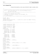
Page 161: ...B 0x00 0x00 0x00 0x00 0x00 0x00 0x00 0x00 0xFF 0x03 0x00 0x00 0x00 0x00 0x00 0x00 0x00 0x00 0x00 0x00 0x00 Useful definitions constants and macros to make the sample code easier to follow define MEM_OFFSET 0x01374B0B Location is platform dependent define REG_OFFSET MEM_OFFSET 0xFFE0 Memory offset 64K 0x20 define MEM_SIZE 0xA000 40 kb display buffer typedef unsigned char BYTE Some usefule typedefs ...

Page 162: ...G 0x01 0x23 Register 02h Mode Register 1 4BPP High Performance CLKi 2 SET_REG 0x02 0xB0 Register 03h Mode Register 2 Normal power mode SET_REG 0x03 0x03 Register 04h Horizontal Panel Size 320 pixels 320 8 1 39 27h SET_REG 0x04 0x27 Register 05h Vertical Panel Size LSB 240 pixels Register 06h Vertical Panel Size MSB 240 1 239 EFh SET_REG 0x05 0xEF SET_REG 0x06 0x00 Register 07h FPLINE Start Positio...

Page 163: ...sed by this panel SET_REG 0x0B 0x00 Register 0Ch Screen 1 Start Word Address LSB Register 0Dh Screen 1 Start Word Address MSB Start address should be set to 0 SET_REG 0x0C 0x00 SET_REG 0x0D 0x00 Register 0Fh Screen 2 Start Word Address LSB Register 10h Screen 2 Start Word Address MSB Set this start address to 0 too SET_REG 0x0F 0x00 SET_REG 0x10 0x00 Register 12h Memory Address Offset Used for set...

Page 164: ...to start RGB sequencing at the first LUT entry SET_REG 0x15 0x00 Register 16h Look Up Table Bank Select Set all the banks to 0 At 4BPP this makes no difference however it will affect appearance at other color depths SET_REG 0x16 0x00 Register 17h Look Up Table Data Write 16 RGB triplets to setup the LUT for 4BPP operation The LUT is 16 elements deep 4BPP uses all the idices pLUT Color_4BPP for LUT...

Page 165: ...REG 0x1B 0x00 Register 1Ch Line Byte Count set to 0 Not used by landscape mode SET_REG 0x0C 0x00 Register 1Fh TestMode set to 0 SET_REG 0x1F 0x00 Draw a 100x100 red rectangle in the upper left corner 0 0 of the display for y 0 y 100 y Set the memory pointer at the start of each line Pointer MEM_OFFSET Y Line_Width BPP 8 X BPP 8 pMem LPBYTE MEM_OFFSET y 320 BitsPerPixel 8 0 for x 0 x 100 x 2 pMem 0...

Page 166: ... tmp 1 while Height 1 tmp tmp Height 1 tmp OffsetBytes Height BitsPerPixel 8 Set 1 Line Byte Count to size of the ROTATED width i e current height 2 Start Address to the offset of the width of the ROTATED display in SwivelView mode the start address registers point to bytes SET_REG 0x1C BYTE OffsetBytes OffsetBytes SET_REG 0x0C LOBYTE OffsetBytes SET_REG 0x0D HIBYTE OffsetBytes Set SwivelView mode...

Page 167: ...A G 002 03 Set the memory pointer at the start of each line Pointer MEM_OFFSET Y Line_Width BPP 8 X BPP 8 NOTICE that in SwivelView mode we will use a value of 256 for the line width value not 240 x 110 pMem LPBYTE MEM_OFFSET y 256 BitsPerPixel 8 x BitsPerPixel 8 for x 110 x 210 x 2 pMem 0x11 Draws 2 pixels in LUT color 1 pMem ...

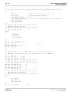
Page 168: ... _HAL_H_ define _HAL_H_ pragma warning disable 4001 Disable the single line comment warning include hal_regs h typedef unsigned char BYTE typedef unsigned short WORD typedef unsigned long DWORD typedef unsigned int UINT typedef int BOOL ifdef INTEL typedef BYTE far LPBYTE typedef WORD far LPWORD typedef UINT far LPUINT typedef DWORD far LPDWORD else typedef BYTE LPBYTE typedef WORD LPWORD typedef ...

Page 169: ... define DEFAULT0 define LANDSCAPE 1 define PORTRAIT2 ifndef NULL ifdef __cplusplus define NULL 0 else define NULL void 0 endif endif SIZE_VERSION is the size of the version string eg 1 00 SIZE_STATUS is the size of the status string eg b for beta SIZE_REVISION is the size of the status revision string eg 00 define SIZE_VERSION5 define SIZE_STATUS 2 define SIZE_REVISION3 ifdef ENABLE_DPF Debug_prin...

Page 170: ...d define PRODUCT_ID 0x18 enum ID_UNKNOWN ID_S1D13704 ID_S1D13704F00A define MAX_MEM_ADDR 40960 1 define FORTY_K 40960 define MAX_DEVICE 10 define SE_RSVD 0 DetectEndian is used to determine whether the most significant and least significant bytes are reversed by the given compiler define ENDIAN 0x1234 define REV_ENDIAN 0x3412 Definitions for Internal calculations define MIN_NON_DISP_X 32 define MA...

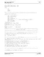
Page 171: ...pedef HAL_STRUCT LPHAL_STRUCT endif FUNCTION PROTO TYPES Initialization int seRegisterDevice const LPHAL_STRUCT lpHalInfo int Device int seSetInit int device int seInitHal void Miscellaneous int seGetId int nDevID int pId void seGetHalVersion const char pVersion const char pStatus const char pSta tusRevision int seSetBitsPerPixel int nDevID int nBitsPerPixel int seGetBitsPerPixel int nDevID int pB...

Page 172: ...D val DWORD count int seWriteDisplayDwords int nDevID DWORD addr DWORD val DWORD count Power Save int seHWSuspend int nDevID BOOL val int seSetPowerSaveMode int nDevID int PowerSaveMode Drawing int seSetPixel int nDevID int x int y DWORD color int seGetPixel int nDevID int x int y DWORD pVal int seDrawLine int nDevID int x1 int y1 int x2 int y2 DWORD color int seDrawRect int nDevID int x1 int y1 i...

Page 173: ...HAL_STRUCT Information generated by 1374CFG EXE Copyright c 1998 Seiko Epson Corp All rights reserved Include this file ONCE in your primary source file HAL_STRUCT HalInfo 1374 HAL EXE ID string 0x1234 Detect Endian sizeof HAL_STRUCT Size 0x00 0x23 0xB0 0x03 0x27 0xEF 0x00 0x00 0x1E 0x00 0x3B 0x00 0x00 0x00 0x00 0x00 0x00 0x00 0x00 0xFF 0x03 0x00 0x00 0x00 0x00 0x00 0x00 0x00 0x00 0x00 0x00 0x00 2...

Page 174: ...define REG_MOD_RATE 0x0B define REG_SCRN1_START_ADDR_LSB 0x0C define REG_SCRN1_START_ADDR_MSB 0x0D define REG_RESERVED_1 0x0E define REG_SCRN2_START_ADDR_LSB 0x0F define REG_SCRN2_START_ADDR_MSB 0x10 define REG_RESERVED_2 0x11 define REG_PITCH_ADJUST 0x12 define REG_SCRN1_VERT_SIZE_LSB 0x13 define REG_SCRN1_VERT_SIZE_MSB 0x14 define REG_LUT_ADDR 0x15 define REG_LUT_BANK_SELECT 0x16 define REG_LUT_...

Page 175: ... Design Center Programming Notes and Examples S1D13704 Issue Date 01 02 12 X26A G 002 03 Appendix A Supported Panel Values A 1 Introduction Future versions of this document will supply example tables for programming the S1D13704 for different panels ...

Page 176: ...Page 80 Epson Research and Development Vancouver Design Center S1D13704 Programming Notes and Examples X26A G 002 03 Issue Date 01 02 12 THIS PAGE LEFT BLANK ...

Page 177: ...EEN 1 VERTICAL SIZE REGISTER LSB IO address FFF3h RW Screen 1 Vertical Size REG 13h REG 14h Bit 7 Bit 6 Bit 5 Bit 4 Bit 3 Bit 2 Bit 1 Bit 0 REG 14h SCREEN 1 VERTICAL SIZE REGISTER MSB IO address FFF4h RW n a n a n a n a n a n a Screen 1 Vertical Size Bit 9 Bit 8 REG 15h LOOK UP TABLE ADDRESS REGISTER 7 IO address FFF5h RW n a n a RGB Index Look Up Table Address Bit 1 Bit 0 Bit 3 Bit 2 Bit 1 Bit 0 ...

Page 178: ...S1D13704 Register Summary X26A R 001 03 Page 2 01 02 12 ...

Page 179: ...ment but only for your own use in evaluating Seiko Epson EPSON products You may not modify the document Epson Research and Development Inc disclaims any representation that the contents of this document are accurate or current The Programs Technologies described in this document may contain material protected under U S and or International Patent laws EPSON is a registered trademark of Seiko Epson...

Page 180: ...Page 2 Epson Research and Development Vancouver Design Center S1D13704 13704CFG EXE Configuration Program X26A B 001 02 Issue Date 01 02 08 THIS PAGE LEFT BLANK ...

Page 181: ...laneous Options 10 System 11 LUT Control 12 Open 13 Save 14 Help 15 Exit 15 Comments 16 List of Figures Figure 1 13704CFG Window 7 Figure 2 Panel Information 8 Figure 3 Miscellaneous Options 10 Figure 4 System Options 11 Figure 5 ERROR Frame Rate 11 Figure 6 ERROR Zero Frame Rate 12 Figure 7 LUT Control 12 Figure 8 13704CFG File Open Dialog 13 Figure 9 ERROR Unable to read HAL 14 Figure 10 13704CF...

Page 182: ...Page 4 Epson Research and Development Vancouver Design Center S1D13704 13704CFG EXE Configuration Program X26A B 001 02 Issue Date 01 02 08 THIS PAGE LEFT BLANK ...

Page 183: ...el types clock rates color depths etc for S1D13704 demonstration programs 13704CFG can Read programs based on the 13704 Hardware Abstraction Layer HAL modify the settings and write the changes back to the file The ability to read modify and write bypasses having to recompile after every change Write C header files containing register settings which can be used to initialize the 13704 registers in ...

Page 184: ...allation There is no installation program for 13704CFG Installation to a local drive is done by copying 13704CFG EXE and 13704CFG HLP to your hard drive and optionally creating a link on the Windows desktop for easy access to the program Usage Open the drive and folder where you copied 13704CFG EXE and double click the icon to start the program Optionally if you created a link to the program on yo...

Page 185: ...D13704 Issue Date 01 02 08 X26A B 001 02 13704CFG The 13704CFG window has four main sections Panel information includes Dimensions LookUp Table Miscellaneous Options and System settings Figure 1 13704CFG Window The following sections describe each of the main sections of the configuration dialog box ...

Page 186: ...selected STN TFT select STN for passive panels or TFT for active panels Switching between these two panel types causes visible changes to take place to the configuration dialog box 4 Bit 8 Bit here the panel data width is selected When STN panel types are selected the options are 4 bit and 8 bit When TFT panels are selected the options will be 9 bit and 12 bit Dimensions in the left selection box ...

Page 187: ...eriod is roughly one hour When not selected the modulated image is never consecutively repeated This option is STN specific and is disabled if TFT is selected MOD Count the mod count value specifies the number of FPLINEs between toggles of the MOD output signal When set to 0 default the MOD output signal toggles every FPFRAME This field is for passive panels only and is generally only required for...

Page 188: ... Video Invert is not availlable for TFT operation HW Power Save Enable the S1D13704 supports two power save modes One is initi ated by software the second in response to input on the GPIO0 pin In order for the hardware power save mode to function this option must be selected High Performance improves chip throughput at the expense of power consumption When not selected the internal MCLK signal is ...

Page 189: ...ms System The options in the System section describe the items which are required for frame rate calculations and where in CPU address space the S1D13704 will be located Figure 4 System Options Memory Location this describes where in CPU address space the S1D13704 will be located This setting is required by the HAL to locate the S1D13704 If the settings from 13704CFG will be saved to a C header fi...

Page 190: ... the clock rate being applied to the S1D13704 in kHz LUT Control The items in this section control the color depth for the S1D13704 after initialization Figure 7 LUT Control The color depth selections in this section will become enabled or disabled in response to the panel dimensions entered i e there is only enough memory to operate a 640x480 panel at 1 bit per pixel so the selections for 2 BPP 4...

Page 191: ...ller numerical value in display memory may be displayed with a greater intensity than a larger value When the lookup table is bypassed the colors displayed on the panel are directly propor tional to their memory value i e at 4 bit per pixel 00h will display as black and 0Fh will display as full intensity Open Click on the Open button to read the settings saved in an executable program based on the...

Page 192: ...ure 9 ERROR Unable to read HAL Save Click on the Close button to save the current configuration settings When clicked the standard Windows file Save As dialog box is displayed Figure 10 13704CFG Save As Dialog From the save as dialog box first select the type of file to save to in the Save as type edit field 13704CFG currently saves in three file formats EXE files are binary images containing a HA...

Page 193: ...ready exist and be an S1D13704 HAL based program 13704CFG is cannot save to a non existent program If 13704CFG is unable to locate the HAL information in the file being saved to the following dialog box is displayed Figure 11 ERROR Unable to read HAL Help Clicking on the Help button will start the help file for S1D13704CFG Exit Clicking on the Exit button exits 13704CFG immediately The user is not...

Page 194: ...1 02 Issue Date 01 02 08 Comments It is assumed that the 13704CFG user is familiar with S1D13704 hardware and software Refer to the S1D13704 Functional Hardware Specification drawing office number X22A A 001 xx and the S1D13704 Programming Notes and Examples manual drawing office number X22A G 002 xx for information ...

Page 195: ...ent but only for your own use in evaluating Seiko Epson EPSON products You may not modify the document Epson Research and Development Inc disclaims any representation that the contents of this document are accurate or current The Programs Technologies described in this document may contain material protected under U S and or International Patent laws EPSON is a registered trademark of Seiko Epson ...

Page 196: ...Page 2 Epson Research and Development Vancouver Design Center S1D13704 13704SHOW Demonstration Program X26A B 002 02 Issue Date 01 02 08 THIS PAGE LEFT BLANK ...

Page 197: ...s done by a serial communication link Alternative methods include EPROM parallel port connection or network connection It is beyond the scope of this document to provide support for target host configurations S1D13704 Supported Evaluation Platforms 13704SHOW has been tested with the following S1D13704 supported evaluation platforms PC system with an Intel 80x86 processor M68332BCC Business Card Co...

Page 198: ...oinit bypass register initialization and use values which are currently in the registers displays the help screen Program Messages ERROR Too many devices registered There are too many display devices attached to the HAL The HAL currently can manage only one device ERROR Could not register 13704 device A 13704 device was not found at the configured addresses Check the configuration address using th...

Page 199: ... but only for your own use in evaluating Seiko Epson EPSON products You may not modify the document Epson Research and Development Inc disclaims any representation that the contents of this document are accurate or current The Programs Technologies described in this document may contain material protected under U S and or International Patent laws EPSON is a registered trademark of Seiko Epson Cor...

Page 200: ...Page 2 Epson Research and Development Vancouver Design Center S1D13704 13704SPLT Display Utility X26A B 003 02 Issue Date 01 02 08 THIS PAGE LEFT BLANK ...

Page 201: ...nts the model employed is that of host target It is assumed that the system has a means of downloading software from the host to the target platform Typically this is done by a serial communication link Alternative methods include EPROM parallel port connection or network connection It is beyond the scope of this document to provide support for target host configurations S1D13704 Supported Evaluat...

Page 202: ...y the help screen After starting 13704SPLT the following keyboard commands are available Manual mode u move Screen 2 up d move Screen 2 down HOME covers Screen 1 with Screen 2 END displays only Screen 1 Automatic mode any key change the direction of split screen movement for PC only Both modes b changes the color depth bits per pixel ESC exits 13704SPLT 13704SPLT Example 1 Type 13704splt a to auto...

Page 203: ...d to the HAL The HAL currently can manage only one device ERROR Could not register 13704 device A 13704 device was not found at the configured addresses Check the configuration address using the 13704CFG configuration program ERROR Did not detect 13704 The HAL was unable to read the revision code register on the S1D13704 Ensure that the S1D13704 hardware is installed and that the hardware platform...

Page 204: ...Page 6 Epson Research and Development Vancouver Design Center S1D13704 13704SPLT Display Utility X26A B 003 02 Issue Date 01 02 08 THIS PAGE LEFT BLANK ...

Page 205: ... but only for your own use in evaluating Seiko Epson EPSON products You may not modify the document Epson Research and Development Inc disclaims any representation that the contents of this document are accurate or current The Programs Technologies described in this document may contain material protected under U S and or International Patent laws EPSON is a registered trademark of Seiko Epson Cor...

Page 206: ...Page 2 Epson Research and Development Vancouver Design Center S1D13704 13704VIRT Display Utility X26A B 004 02 Issue Date 01 02 08 THIS PAGE LEFT BLANK ...

Page 207: ...tware from the host to the target platform Typically this is done by a serial communication link Alternative methods include EPROM parallel port connection or network connection It is beyond the scope of this document to provide support for target host configurations S1D13704 Supported Evaluation Platforms 13704VIRT has been tested with the following S1D13704 supported evaluation platforms PC syst...

Page 208: ...y width which includes both on screen and off screen size the maximum virtual display width for each display mode is 1 bpp 4096 pixels 2 bpp 2048 pixels 4 bpp 1024 pixels 8 bpp 512 pixels The following keyboard commands are for navigation within the program Manual mode scrolls up scrolls down pans to the left pans to the right HOME moves the display screen so that the upper right of the virtual sc...

Page 209: ...el 4 Press ESC to exit the program Program Messages ERROR Too many devices registered There are too many display devices attached to the HAL The HAL currently can manage only one device ERROR Could not register 13704 device A 13704 device was not found at the configured addresses Check the configuration address using the 13704CFG configuration program ERROR Did not detect 13704 The HAL was unable ...

Page 210: ...Page 6 Epson Research and Development Vancouver Design Center S1D13704 13704VIRT Display Utility X26A B 004 02 Issue Date 01 02 08 THIS PAGE LEFT BLANK ...

Page 211: ...t but only for your own use in evaluating Seiko Epson EPSON products You may not modify the document Epson Research and Development Inc disclaims any representation that the contents of this document are accurate or current The Programs Technologies described in this document may contain material protected under U S and or International Patent laws EPSON is a registered trademark of Seiko Epson Co...

Page 212: ...Page 2 Epson Research and Development Vancouver Design Center S1D13704 13704PLAY Diagnostic Utility X26A B 005 03 Issue Date 01 02 08 THIS PAGE LEFT BLANK ...

Page 213: ...gram 13704CFG EXE which can be used to configure 13704PLAY This software is designed to work with a variety of embedded and personal computer PC environments For embedded environments the model employed is that of host target It is assumed that the system has a means of downloading software from the host to the target platform Typically this is done by a serial communication link Alternative metho...

Page 214: ...otherwise the register is read XA Reads all registers L index data1 data2 data3 Reads writes Look Up Table LUT values Writes data to the LUT index when data is specified otherwise the LUT index is read Data must consist of 3 bytes 1 red 1 green 1 blue and range in value from 0x00 to 0x0F LA Reads all LUT values F W addr1 addr2 data Fills bytes or words from address 1 to address 2 with data Data ca...

Page 215: ...ring long read operations to prevent data from scrolling off the display Set 0 to disable Q Quits this utility Displays Help information 13704PLAY Example 1 Type 13704PLAY to start the program 2 Type for help 3 Type i to initialize the registers 4 Type xa to display the contents of the registers 5 Type x 5 to read register 5 6 Type x 3 10 to write 10 hex to register 3 7 Type f 0 400 aa to fill the...

Page 216: ...mi colon is used as a comment delimitor Everything on a line after the semi colon will be ignored On a PC platform a typical script command line is 13704PLAY dumpregs scr results This causes the script file dumpregs scr to be interpreted and the results to be sent to the file results Example 1 The script file dumpregs scr can be created with and text editor and will look like the following This fi...

Page 217: ...tered There are too many display devices attached to the HAL The HAL currently can manage only one device ERROR Could not register 13704 device A 13704 device was not found at the configured addresses Check the configuration address using the 13704CFG configuration program WARNING Did not detect 13704 The HAL did not detect an S1D13704 however 13704PLAY will continue to function ...

Page 218: ...Page 8 Epson Research and Development Vancouver Design Center S1D13704 13704PLAY Diagnostic Utility X26A B 005 03 Issue Date 01 02 08 THIS PAGE LEFT BLANK ...

Page 219: ...nt but only for your own use in evaluating Seiko Epson EPSON products You may not modify the document Epson Research and Development Inc disclaims any representation that the contents of this document are accurate or current The Programs Technologies described in this document may contain material protected under U S and or International Patent laws EPSON is a registered trademark of Seiko Epson C...

Page 220: ...Page 2 Epson Research and Development Vancouver Design Center S1D13704 13704BMP Demonstration Program X26A B 006 02 Issue Date 01 02 08 THIS PAGE LEFT BLANK ...

Page 221: ...MP is not supported on non PC platforms Installation Copy the file 13704BMP EXE to a directory that is in the DOS path on your hard drive Usage At the prompt type 13704bmp bmp_file a time l p Where bmp_file the name of the file to display a time automatic mode returns to the operating system after time seconds If time is not specified the default is 5 seconds This option is intended for use with b...

Page 222: ...hed to the HAL The HAL currently can manage only one device ERROR Could not register 13704 device A 13704 device was not found at the configured addresses Check the configuration address using the 13704CFG configuration program ERROR Did not detect 13704 The HAL was unable to read the revision code register on the S1D13704 Ensure that the S1D13704 hardware is installed and that the hardware platfo...

Page 223: ...ent but only for your own use in evaluating Seiko Epson EPSON products You may not modify the document Epson Research and Development Inc disclaims any representation that the contents of this document are accurate or current The Programs Technologies described in this document may contain material protected under U S and or International Patent laws EPSON is a registered trademark of Seiko Epson ...

Page 224: ...Page 2 Epson Research and Development Vancouver Design Center S1D13704 13704PWR Power Save Utility X26A B 007 02 Issue Date 01 02 08 THIS PAGE LEFT BLANK ...

Page 225: ...Typically this is done by serial communications where the PC uses a terminal program to send control commands and information to the target processor Alternatively the PC can program an EPROM which is then placed in the target platform Some target platforms can also communicate with the PC via a parallel port connection or an Ethernet connection S1D13704 Supported Evaluation Platforms 13704PWR has...

Page 226: ...displays this usage message Program Messages ERROR Unknown command line argument An invalid command line argument was entered Enter a valid command line argument ERROR Too many devices registered There are too many display devices attached to the HAL The HAL currently can manage only one device ERROR Could not register 13704 device A 13704 device was not found at the configured addresses Check the...

Page 227: ...uating Seiko Epson EPSON products You may not modify the document Epson Research and Development Inc disclaims any representation that the contents of this document are accurate or current The Programs Technologies described in this document may contain material protected under U S and or International Patent laws EPSON is a registered trademark of Seiko Epson Corporation Microsoft and Windows is ...

Page 228: ...Page 2 Epson Research and Development Vancouver Design Center S1D13704 Windows CE Display Drivers X26A E 001 02 Issue Date 01 02 08 THIS PAGE LEFT BLANK ...

Page 229: ...ons below 1 Install Microsoft Windows NT v4 0 2 Install Microsoft Visual C C v5 0 3 Install the Microsoft Windows CE Embedded Toolkit ETK by running SETUP EXE from the ETK compact disc 1 4 Create a new project by following the procedure documented in Creating a New Project Directory from the Windows CE ETK Alternately use the current DEMO7 project included with the ETK Follow the steps below to cr...

Page 230: ...ed in X wince platform cepc files where X is the drive letter Since the S5U13704B00C maps the 64K byte region from D0000h to DFFFFh make sure no other devices occupy this area The following lines should be in CON FIG BIB NK 80200000 00500000 RAMIMGE RAM 80700000 00500000 RAM Note DISPDRVR C should include the following define PhysicalPortAddr 0x000DF000L define PhysicalVmemAddr 0x000D0000L 5 Edit ...

Page 231: ...loppy drive or a hard drive The two methods are described below To load CEPC from a floppy drive 1 Create a DOS bootable floppy disk 2 Edit CONFIG SYS on the floppy disk to contain the following line only device a himem sys 3 Edit AUTOEXEC BAT on the floppy disk to contain the following lines mode com1 9600 n 8 1 loadcepc B 9600 C 1 c wince release nk bin 4 Copy LOADCEPC EXE from c wince public co...

Page 232: ... Date 01 02 08 1 4 Comments At the time of this printing the drivers have been tested on the x86 CPUs and have only been run with version 2 0 of the ETK We are constantly updating the drivers so please check our website at www erd epson com or contact your Seiko Epson or Epson Electronics America sales representative ...

Page 233: ...nd use this document but only for your own use in evaluating Seiko Epson EPSON products You may not modify the document Epson Research and Development Inc disclaims any representation that the contents of this document are accurate or current The Programs Technologies described in this document may contain material protected under U S and or International Patent laws EPSON is a registered trademar...

Page 234: ...Page 2 Epson Research and Development Vancouver Design Center S1D13704 S5U13704B00C Rev 1 0 ISA Bus Evaluation Board User Manual X26A G 005 03 Issue Date 01 02 12 THIS PAGE LEFT BLANK ...

Page 235: ...Description 14 6 1 ISA Bus Support 14 6 1 1 Display Adapter Card Support 14 6 1 2 Expanded Memory Manager 14 6 2 Non ISA Bus Support 15 6 3 Embedded Memory Support 15 6 4 Decode Logic 15 6 5 Clock Input Support 16 6 6 LCD Panel Voltage Setting 16 6 7 Monochrome LCD Panel Support 16 6 8 Color Passive LCD Panel Support 16 6 9 Color TFT D TFD LCD Panel Support 16 6 10 Power Save Modes 17 6 11 Adjusta...

Page 236: ...Page 4 Epson Research and Development Vancouver Design Center S1D13704 S5U13704B00C Rev 1 0 ISA Bus Evaluation Board User Manual X26A G 005 03 Issue Date 01 02 12 THIS PAGE LEFT BLANK ...

Page 237: ...t Bus Selection 8 Table 2 3 Jumper Settings 9 Table 3 1 LCD Signal Connector J5 Pinout 10 Table 4 1 CPU BUS Connector H1 Pinout 11 Table 4 2 CPU BUS Connector H2 Pinout 12 Table 5 1 Host Bus Interface Pin Mapping 13 List of Figures Figure 8 1 S1D13704B00C Schematic Diagram 1 of 4 20 Figure 8 2 S1D13704B00C Schematic Diagram 2 of 4 21 Figure 8 3 S1D13704B00C Schematic Diagram 3 of 4 22 Figure 8 4 S...

Page 238: ...Page 6 Epson Research and Development Vancouver Design Center S1D13704 S5U13704B00C Rev 1 0 ISA Bus Evaluation Board User Manual X26A G 005 03 Issue Date 01 02 12 THIS PAGE LEFT BLANK ...

Page 239: ...Hardware Functional Specification document number X26A A 001 xx 1 1 Features 80 pin QFP14 package SMT technology for all appropriate devices 4 8 bit monochrome and color passive LCD panel support 9 12 bit LCD TFT D TFD panel support Selectable 3 3V or 5 0V LCD panel support Oscillator support for CLKI up to 50MHz with internal clock divide or 25MHz with no internal clock divide Embedded 40K byte S...

Page 240: ...us Table 2 1 Configuration DIP Switch Settings Switch Signal Closed 0 or low Open 1 or high SW1 1 CNF0 See Host Bus Selection table below See Host Bus Selection table below SW1 2 CNF1 SW1 3 CNF2 SW1 4 CNF3 Little Endian Big Endian SW1 5 CNF4 Active low LCDPWR signal Active high LCDPWR signal SW1 6 GPIO0 Hardware Suspend Disable Hardware Suspend Enable recommended settings configured for ISA bus su...

Page 241: ...01 02 12 X26A G 005 03 Table 2 3 Jumper Settings Description 1 2 2 3 JP1 IOVDD Selection 5 0V IOVDD 3 3V IOVDD JP2 RD WR Signal Selection Pulled up to IOVDD No Connection JP3 BS Signal Selection Pulled up to IOVDD No Connection JP4 LCD Panel Voltage Selection 5 0V LCD Panel 3 3V LCD Panel recommended settings configured for ISA bus support ...

Page 242: ...5 D5 D1 D5 UD1 UD1 G0 G1 BFPDAT6 13 D2 D6 D6 D2 D6 UD2 UD2 B2 B3 BFPDAT7 15 D3 D7 D7 D3 D7 UD3 UD3 B1 B2 BFPDAT8 17 B0 B1 BFPDAT9 19 R0 BFPDAT10 21 G0 BFPDAT11 23 B0 BFPSHIFT 33 FPSHIFT FPSHIFT FPSHIFT FPSHIFT FPSHIFT FPSHIFT FPSHIFT FPSHIFT FPSHIFT BFPSHIFT2 35 FPSHIFT2 BFPLINE 37 FPLINE FPLINE FPLINE FPLINE FPLINE FPLINE FPLINE FPLINE FPLINE BFPFRAME 39 FPFRAME FPFRAME FPFRAME FPFRAME FPFRAME FP...

Page 243: ...ed to DB7 of the S1D13704 11 GND Ground 12 GND Ground 13 SD8 Connected to DB8 of the S1D13704 14 SD9 Connected to DB9 of the S1D13704 15 SD10 Connected to DB10 of the S1D13704 16 SD11 Connected to DB11 of the S1D13704 17 GND Ground 18 GND Ground 19 SD12 Connected to DB12 of the S1D13704 20 SD13 Connected to DB13 of the S1D13704 21 SD14 Connected to DB14 of the S1D13704 22 SD15 Connected to DB15 of...

Page 244: ...e S1D13704 12 SA9 Connected to AB9 of the S1D13704 13 SA10 Connected to AB10 of the S1D13704 14 SA11 Connected to AB11 of the S1D13704 15 SA12 Connected to AB12 of the S1D13704 16 SA13 Connected to AB13 of the S1D13704 17 GND Ground 18 GND Ground 19 SA14 Connected to AB14 of the S1D13704 20 SA15 Connected to AB14 of the S1D13704 21 SA16 Connected to AB16 of the S1D13704 22 SA17 Connected to AB17 o...

Page 245: ...B 15 1 A 15 1 A 15 1 A 15 1 A 15 1 A 15 1 A 15 1 AB0 A0 A0 LDS A0 A0 A0 DB 15 0 D 15 0 D 15 0 D 15 0 D 15 0 D 15 0 D 15 0 WE1 WE1 WE1 UDS DS WE1 BHE CS CSn CSn External Decode External Decode External Decode External Decode BCLK CKIO CKIO BCLK BCLK BCLK BCLK BS BS BS AS AS Connect to VSS Connect to IO VDD RD WR RD WR RD WR R W R W RD1 Connect to IO VDD RD RD RD Connect to IO VDD SIZ1 RD0 RD WE0 WE...

Page 246: ...imary Display Adapter VGA or Monochrome the following applies ISA or VL Bus VGA Display Adapter When the S5U13704B00B board is used with an ISA or VL Bus VGA display adapter the VGA card must have a 16 bit BIOS to prevent conflicts during 16 bit accesses MEMCS16 If an 8 bit VGA adapter card is installed in the system being used it must be removed and the screen display routed through a COM port to...

Page 247: ...3704 CS pin 74 RESET pin 73 and other decode logic signals for ISA bus use This functionality must now be provided externally remove the PAL from its socket to eliminate conflicts resulting from two different outputs driving the same input Refer to Table 5 1 Host Bus Interface Pin Mapping for connection details Note When using a 3 3V host bus interface IOVDD must be set to 3 3V by setting jumper J...

Page 248: ...CD panels All necessary signals are provided on the 40 pin ribbon cable header J5 The interface signals on the cable are alternated with grounds to reduce crosstalk and noise Refer to Table 3 1 LCD Signal Connector J5 Pinout on page 10 for specific connection information 6 8 Color Passive LCD Panel Support The S1D13704 directly supports 4 and 8 dual and single color passive LCD panels All the nece...

Page 249: ...al which is configurable as active high or active low by the CNF4 signal status on the rising edge of the RESET signal For the proper operation of the VLCD power supply LCDPWR must be configured as active low Determine the panel s specific power requirements and set the potentiometer accordingly before connecting the panel 6 12 Adjustable LCD Panel Positive Power Supply Most color passive LCD pane...

Page 250: ... H1 and H2 for easy interface to a CPU Bus other than ISA Refer to Table 4 1 CPU BUS Connector H1 Pinout on page 11 and Table 4 2 CPU BUS Connector H2 Pinout on page 12 for specific settings Note These headers only provide the CPU Bus interface signals from the S1D13704 When another host bus interface is selected by CNF 3 0 and BS appropriate external decode logic MUST be used to access the S1D137...

Page 251: ...ers 13 1 J5 CON40A Shrouded header 2x20 PTH center key 14 1 L1 1µH MCI 1812 inductor 15 3 L2 L4 Ferrite bead Philips BDS3 3 8 9 4S2 16 1 Q1 2N3906 PNP signal transistor SOT23 17 1 Q2 2N3903 NPN signal transistor SOT23 18 6 R1 R6 15K 5 0805 resistor 19 7 R7 R13 10K 5 0805 resistor 20 1 R14 470K 5 0805 resistor 21 1 R15 200K 200K Trim POT Spectrol 63S204T607 or equivalent 22 1 R16 14K 1 0805 resisto...

Page 252: ...uF C7 0 1uF C5 0 1uF JP3 HEADER 3 1 2 3 JP2 HEADER 3 1 2 3 R4 15K R3 15K R2 15K R1 15K R5 15K C2 0 1uF C4 0 1uF C3 0 1uF JP1 HEADER 3 1 2 3 R6 15K S1 SW DIP 6 1 2 3 4 5 6 12 11 10 9 8 7 U1 S1D13704F00A 70 69 68 67 66 65 64 63 62 59 58 57 56 55 54 53 37 36 35 34 32 31 30 74 43 61 20 40 72 60 50 27 80 19 18 17 16 15 14 13 12 11 9 8 7 6 5 4 3 33 49 48 47 46 45 79 78 77 76 75 73 51 71 2 44 1 21 10 41 ...

Page 253: ...BDRDY FPLINE BFPFRAME BFPSHIFT LCDPWR BFPLINE 12V VDDH VLCD VCC VCC VCC VCC 12V 12V 3 3V VCC J5 CON40A 1 3 5 7 9 11 13 15 17 19 21 23 25 27 29 31 33 35 37 39 2 4 6 8 10 12 14 16 18 20 22 24 26 28 30 32 34 36 38 40 U3 74AHC244 2 18 4 16 6 14 8 12 11 9 13 7 15 5 17 3 1 19 20 10 1A1 1Y1 1A2 1Y2 1A3 1Y3 1A4 1Y4 2A1 2Y1 2A2 2Y2 2A3 2Y3 2A4 2Y4 1G 2G VCC GND U4 74AHC244 2 18 4 16 6 14 8 12 11 9 13 7 15 ...

Page 254: ...27 28 29 30 31 IOCHCK SD7 SD6 SD5 SD4 SD3 SD2 SD1 SD0 IOCHRDY AEN SA19 SA18 SA17 SA16 SA15 SA14 SA13 SA12 SA11 SA10 SA9 SA8 SA7 SA6 SA5 SA4 SA3 SA2 SA1 SA0 J2 AT CON B 1 2 3 4 5 6 7 8 9 10 11 12 13 14 15 16 17 18 19 20 21 22 23 24 25 26 27 28 29 30 31 GND RESET 5V IRQ9 5V DRQ2 12V OWS 12V GND SMEMW SMEMR IOW IOR DACK3 DRQ3 DACK1 DRQ1 REFRESH CLK IRQ7 IRQ6 IRQ5 IRQ4 IRQ3 DACK2 T C BALE 5V OSC GND J...

Page 255: ... Friday October 09 1998 Size Document Number Rev Date Sheet of PSVCC PSVCC VCC PSIOVDD PSVCC PSVCC IOVDD PSIOVDD VLCD VDDH C20 4 7uF 50V R18 1K R19 100K R20 100K Q2 2N3903 2 1 3 R14 470K R15 200K 1 3 2 R16 14K C18 4 7uF 50V C19 4 7uF 50V C21 47uF 16V C22 56uF 35V Low ESR C17 47uF 16V R17 1K R21 100K 1 3 2 U9 RD 0412 1 2 3 4 5 6 7 8 9 10 11 12 VOUT_ADJ DC_IN REMOTE GND GND GND GND GND NC GND GND DC...

Page 256: ...Page 24 Epson Research and Development Vancouver Design Center S1D13704 S5U13704B00C Rev 1 0 ISA Bus Evaluation Board User Manual X26A G 005 03 Issue Date 01 02 12 THIS PAGE LEFT BLANK ...

Page 257: ...this document but only for your own use in evaluating Seiko Epson EPSON products You may not modify the document Epson Research and Development Inc disclaims any representation that the contents of this document are accurate or current The Programs Technologies described in this document may contain material protected under U S and or International Patent laws EPSON is a registered trademark of Se...

Page 258: ...Page 2 EPSON Research and Development Vancouver Design Center S1D13704 Interfacing to the Toshiba MIPS TX3912 Processor X26A G 004 02 Issue Date 01 02 12 THIS PAGE LEFT BLANK ...

Page 259: ...to the Toshiba TX3912 8 2 1 General Description 8 2 2 Memory Mapping and Aliasing 9 2 3 S1D13704 Configuration and Pin Mapping 9 3 System Design Using the ITE IT8368E PC Card Buffer 10 3 1 Hardware Description 10 3 2 IT8368E Configuration 11 3 3 Memory Mapping and Aliasing 12 3 4 S1D13704 Configuration 13 4 Software 14 5 Technical Support 15 5 1 EPSON LCD Controllers S1D13704 15 5 2 Toshiba MIPS T...

Page 260: ...Page 4 EPSON Research and Development Vancouver Design Center S1D13704 Interfacing to the Toshiba MIPS TX3912 Processor X26A G 004 02 Issue Date 01 02 12 THIS PAGE LEFT BLANK ...

Page 261: ...ble 2 2 S1D13704 Generic 2 Interface Pin Mapping 9 Table 3 1 TX3912 to Unbuffered PC Card Slots System Address Mapping 12 Table 3 2 TX3912 to PC Card Slots Address Remapping Using the IT8368E 12 Table 3 3 S1D13704 Configuration Using the IT8368E 13 Table 3 4 S1D13704 Generic 1 Interface Pin Mapping 13 List of Figures Figure 2 1 S1D13704 to TX3912 Direct Connection 8 Figure 3 1 S1D13704 to TX3912 C...

Page 262: ...Page 6 EPSON Research and Development Vancouver Design Center S1D13704 Interfacing to the Toshiba MIPS TX3912 Processor X26A G 004 02 Issue Date 01 02 12 THIS PAGE LEFT BLANK ...

Page 263: ... the TX3912 contact Toshiba or refer to the Toshiba website under semiconductors at http www toshiba com taec nonflash indexproducts html For further information on the ITE IT8368E refer to the IT8368E PC Card GPIO Buffer Chip Specification 1 1 General Description The Toshiba MIPS TX3912 processor supports up to two PC Card PCMCIA slots It is through this host bus interface that the S1D13704 conne...

Page 264: ...tion of the interface Figure 2 1 S1D13704 to TX3912 Direct Connection The Generic 2 host interface control signals of the S1D13704 are asynchronous with respect to the S1D13704 bus clock This gives the system designer full flexibility to choose the appropriate source or sources for CLKI and BCLK The choice of whether both clocks should be the same and whether to use DCLKOUT divided as clock source...

Page 265: ... must be added 2 3 S1D13704 Configuration and Pin Mapping The S1D13704 is configured at power up by latching the state of the CNF 4 0 pins Pin BS also plays a role in host bus interface configuration For details on configuration refer to the S1D13704 Hardware Functional Specification document number X26A A 001 xx The table below shows those configuration settings relevant to the direct connection ...

Page 266: ...t EPSON LCD controllers The ITE IT8368E provides eleven Multi Function IO pins MFIO Configuration registers may be used to allow these MFIO pins to provide the control signals required to implement the S1D13704 CPU interface The TX3912 processor only provides addresses A 12 0 therefore devices requiring more address space must use an external device to latch A 25 13 The IT8368E s MFIO pins can be ...

Page 267: ...provide additional flexibility 3 2 IT8368E Configuration The IT8368E provides eleven multi function IO pins MFIO The IT8368E must have both Fix Attribute IO and VGA modes on When both these modes are enabled the MFIO pins provide control signals needed by the S1D13704 host bus interface and a 16M byte portion of the system PC Card attribute and IO space is allocated to address the S1D13704 When ac...

Page 268: ...ded into Attribute I O and S1D13704 access Table 3 2 TX3912 to PC Card Slots Address Remapping Using the IT8368E provides all details of the Attribute IO address reallocation by the IT8368E Table 3 2 TX3912 to PC Card Slots Address Remapping Using the IT8368E TX3912 Address Size Function CARDnIOEN 0 Function CARDnIOEN 1 0800 0000h 64M byte Card 1 Attribute Card 1 IO 0C00 0000h 64M byte Card 2 Attr...

Page 269: ...nt number X26A A 001 xx The table below shows those configuration settings relevant to this specific interface When the S1D13704 is configured for Generic 1 interface the host interface pins are mapped as in the table below Table 3 3 S1D13704 Configuration Using the IT8368E S1D13704 Configuration Pin Value hard wired on this pin is used to configure 1 IO VDD 0 VSS BS Generic 2 Generic 1 CNF3 Big E...

Page 270: ... is available for both the test utilities and the drivers The test utilities are configurable for different panel types using a program called 1357CFG or by directly modifying the source The Windows CE v2 0 display drivers can be customized by the OEM for different panel types resolutions and color depths only by modifying the source The S1D13704 test utilities and Windows CE v2 0 display drivers ...

Page 271: ...aiwan R O C Epson Taiwan Technology Trading Ltd 10F No 287 Nanking East Road Sec 3 Taipei Taiwan R O C Tel 02 2717 7360 Fax 02 2712 9164 Singapore Epson Singapore Pte Ltd No 1 Temasek Avenue 36 00 Millenia Tower Singapore 039192 Tel 337 7911 Fax 334 2716 North America Epson Electronics America Inc 150 River Oaks Parkway San Jose CA 95134 USA Tel 408 922 0200 Fax 408 922 0238 http www eea epson com...

Page 272: ...Page 16 EPSON Research and Development Vancouver Design Center S1D13704 Interfacing to the Toshiba MIPS TX3912 Processor X26A G 004 02 Issue Date 01 02 12 THIS PAGE LEFT BLANK ...

Page 273: ...nt but only for your own use in evaluating Seiko Epson EPSON products You may not modify the document Epson Research and Development Inc disclaims any representation that the contents of this document are accurate or current The Programs Technologies described in this document may contain material protected under U S and or International Patent laws EPSON is a registered trademark of Seiko Epson C...

Page 274: ...Page 2 Epson Research and Development Vancouver Design Center S1D13704 Power Consumption X26A G 006 02 Issue Date 01 02 12 THIS PAGE LEFT BLANK ...

Page 275: ...the Core and IO sections in the S1D13704 affects power consumption the higher the voltage the higher the consumption Display mode the resolution panel type and color depth affect power consumption The higher the resolution color depth and number of LCD panel signals the higher the power consumption Note If the High Performance option is turned on the power consumption increases to that of 8 bit pe...

Page 276: ... Panel 320x240 4 bit Single Monochrome Black and White 4 Gray Shades 16 Gray Shades 5 29mW 6 86mW 8 15mW 0 3mW 0 43mW 0 55mW 5 59mW 7 29mW 8 70mW 1 58mW1 1 19mW2 2 Input Clock 6MHz LCD Panel 320x240 4 bit Single Color 2 Colors 4 Colors 16 Colors 6 82mW 7 58mW 8 98mW 1 13mW 2 29mW 2 25mW 7 95mW 9 86mW 11 23mW 1 58mW1 1 19mW2 3 Input Clock 25MHz LCD Panel 640x480 8 bit Single Monochrome Black and Wh...

Page 277: ... Total Power Consumption show that S1D13704 power consumption depends on the specific implementation Active Mode power consumption depends on the desired CPU perfor mance and LCD frame rate whereas Power Save Mode consumption depends on the CPU Interface and Input Clock state In a typical design environment the S1D13704 can be configured to be an extremely power efficient LCD Controller with high ...

Page 278: ...Page 6 Epson Research and Development Vancouver Design Center S1D13704 Power Consumption X26A G 006 02 Issue Date 01 02 12 THIS PAGE LEFT BLANK ...

Page 279: ...oad and use this document but only for your own use in evaluating Seiko Epson EPSON products You may not modify the document Epson Research and Development Inc disclaims any representation that the contents of this document are accurate or current The Programs Technologies described in this document may contain material protected under U S and or International Patent laws EPSON is a registered tra...

Page 280: ...Page 2 Epson Research and Development Vancouver Design Center S1D13704 Interfacing to the Motorola MC68328 Dragonball Microprocessor X26A G 007 03 Issue Date 01 02 12 THIS PAGE LEFT BLANK ...

Page 281: ...us Interface 9 3 1 Bus Interface Modes 9 3 2 Generic 1 Interface Mode 10 3 3 MC68K 1 Interface Mode 11 4 MC68328 To S1D13704 Interface 12 4 1 Hardware Description 12 4 1 1 Using The MC68K 1 Host Bus Interface 12 4 1 2 Using The Generic 1 Host Bus Interface 13 4 2 S1D13704 Hardware Configuration 14 4 3 MC68328 Chip Select Configuration 14 5 Software 15 6 References 16 6 1 Documents 16 6 2 Document ...

Page 282: ...Page 4 Epson Research and Development Vancouver Design Center S1D13704 Interfacing to the Motorola MC68328 Dragonball Microprocessor X26A G 007 03 Issue Date 01 02 12 THIS PAGE LEFT BLANK ...

Page 283: ... 01 02 12 X26A G 007 03 List of Tables Table 3 1 Host Bus Interface Pin Mapping 9 Table 4 1 Summary of Power On Reset Options 14 Table 4 2 Host Bus Interface Selection 14 List of Figures Figure 4 1 Typical Implementation of MC68328 to S1D13704 Interface MC68K 1 12 Figure 4 2 Typical Implementation of MC68328 to S1D13704 Interface Generic 1 13 ...

Page 284: ...Page 6 Epson Research and Development Vancouver Design Center S1D13704 Interfacing to the Motorola MC68328 Dragonball Microprocessor X26A G 007 03 Issue Date 01 02 12 THIS PAGE LEFT BLANK ...

Page 285: ... refresh memory the S1D13704 can reduce system power consumption improve image quality and increase system perfor mance as compared to the Dragonball s on chip LCD controller The designs described in this document are presented only as examples of how such interfaces might be implemented This application note will be updated as appropriate Please check the Epson Research and Development Website at...

Page 286: ...3704 with no glue logic However several of the MC68000 bus control signals are multiplexed with IO and interrupt signals on the MC68328 and in many applications it may be desirable to make these pins available for these alternate functions This requirement may be accommodated through use of the Generic 1 interface mode on the S1D13704 2 2 Chip Select Module The MC68328 can generate up to 16 chip s...

Page 287: ...Read Enable Write Enable for each byte Generic 2 External Chip Select shared Read Write Enable for high byte individual Read Write Enable for low byte The S1D13704 latches CNF 2 0 and BS to allow selection of the host bus interface on the rising edge of RESET After releasing reset the bus interface signals assume their selected configuration The following table shows the functions of each host bus...

Page 288: ...t big endian hosts they would connect to the low order data lines The hardware engineer must ensure that CNF3 selects the proper endian mode upon reset Chip Select CS is driven by decoding the high order address lines to select the proper IO or memory address space WE0 and WE1 are write enables for the low order and high order bytes respectively to be driven low when the host CPU is writing data t...

Page 289: ...t the proper IO or memory address space A0 and WE1 are the enables for the low order and high order bytes respectively to be driven low when the host CPU is reading or writing data to the S1D13704 These must be generated by external decode hardware based upon the control outputs from the host CPU RD WR is the read write signal that is driven low when the CPU writes to the S1D13704 and is driven hi...

Page 290: ...s specifically UDS LDS and DTACK In implementations where all of these pins are available for use as bus control pins then the S1D13704 interface is a straightforward implementation of the MC68K 1 host bus interface For further information on this host bus interface refer to the S1D13704 Hardware Functional Specification document number X26A A 001 xx The following diagram shows a typical implement...

Page 291: ...nserts a variable number of wait states depending upon CPU LCD synchronization and the LCD panel display mode WAIT must be inverted using an inverter enabled by CS to make it an active high signal and thus compatible with the MC68328 architecture A single resistor is used to speed up the rise time of the WAIT DTACK signal when terminating the bus cycle The following diagram shows a typical impleme...

Page 292: ...d to control the S1D13704 A 64K byte address space is used with the S1D13704 control registers mapped into the top 32 bytes of the 64K byte block and the 40K bytes of display buffer mapped to the starting address of the block The chip select should have its RO Read Only bit set to 0 and the WAIT field Wait states should be set to 111b to allow the S1D13704 to terminate bus cycles exter nally Table...

Page 293: ...ailable for both the test utilities and the drivers The test utilities are configurable for different panel types using a program called 13704CFG or by directly modifying the source The Windows CE v2 0 display drivers can be customized by the OEM for different panel types resolutions and color depths only by modifying the source The S1D13704 test utilities and Windows CE v2 0 display drivers are a...

Page 294: ...PS WIRELESS products MC68328 html Epson Research and Development Inc S1D13704 Hardware Functional Specification Document Number X26A A 001 xx Epson Research and Development Inc S5U13704B00C Rev 1 0 ISA Bus Evaluation Board User Manual Document Number X26A G 005 xx Epson Research and Development Inc S1D13704 Programming Notes and Examples Document Number X26A G 002 xx 6 2 Document Sources Motorola ...

Page 295: ... 5812 Fax 042 587 5564 http www epson co jp Hong Kong Epson Hong Kong Ltd 20 F Harbour Centre 25 Harbour Road Wanchai Hong Kong Tel 2585 4600 Fax 2827 4346 Taiwan R O C Epson Taiwan Technology Trading Ltd 10F No 287 Nanking East Road Sec 3 Taipei Taiwan R O C Tel 02 2717 7360 Fax 02 2712 9164 Singapore Epson Singapore Pte Ltd No 1 Temasek Avenue 36 00 Millenia Tower Singapore 039192 Tel 337 7911 F...

Page 296: ...Page 18 Epson Research and Development Vancouver Design Center S1D13704 Interfacing to the Motorola MC68328 Dragonball Microprocessor X26A G 007 03 Issue Date 01 02 12 THIS PAGE LEFT BLANK ...

Page 297: ...use this document but only for your own use in evaluating Seiko Epson EPSON products You may not modify the document Epson Research and Development Inc disclaims any representation that the contents of this document are accurate or current The Programs Technologies described in this document may contain material protected under U S and or International Patent laws EPSON is a registered trademark o...

Page 298: ...Page 2 Epson Research and Development Vancouver Design Center S1D13704 Interfacing to the NEC VR4102 Microprocessor X26A G 008 05 Issue Date 01 02 12 THIS PAGE LEFT BLANK ...

Page 299: ...tem Bus 8 2 1 1 Overview 8 2 1 2 LCD Memory Access Cycles 9 3 S1D13704 Host Bus Interface 10 3 1 Bus Interface Modes 10 3 2 Generic 2 Interface Mode 11 4 VR4102 to S1D13704 Interface 13 4 1 Hardware Description 13 4 2 S1D13704 Hardware Configuration 14 4 3 NEC VR4102 Configuration 15 5 Software 16 6 References 17 6 1 Documents 17 6 2 Document Sources 17 7 Technical Support 18 7 1 Epson LCD Control...

Page 300: ...Page 4 Epson Research and Development Vancouver Design Center S1D13704 Interfacing to the NEC VR4102 Microprocessor X26A G 008 05 Issue Date 01 02 12 THIS PAGE LEFT BLANK ...

Page 301: ... S1D13704 Issue Date 01 02 12 X26A G 008 05 List of Tables Table 3 1 Host Bus Interface Pin Mapping 10 Table 4 1 Summary of Power On Reset Options 14 Table 4 2 Host Bus Selection 14 List of Figures Figure 2 1 NEC VR4102 Read Write Cycles 9 Figure 4 1 Typical Implementation of VR4102 to S1D13704 Interface 13 ...

Page 302: ...Page 6 Epson Research and Development Vancouver Design Center S1D13704 Interfacing to the NEC VR4102 Microprocessor X26A G 008 05 Issue Date 01 02 12 THIS PAGE LEFT BLANK ...

Page 303: ...support an external LCD controller and the pairing of these two devices results in an embedded system offering impressive display capability with very low power consumption The designs described in this document are presented only as examples of how such interfaces might be implemented This application note will be updated as appropriate Please check the Epson Research and Development Website at h...

Page 304: ...erface requirements 2 1 1 Overview The NEC VR4102 is designed around the RISC architecture developed by MIPS This microprocessor is designed around the 66MHz VR4100 CPU core which supports 64 bit processing The CPU communicates with the Bus Control Unit BCU with its internal SysAD bus The BCU in turn communicates with external devices with its ADD and DAT buses that can be dynamically sized to 16 ...

Page 305: ...ce Once an address in the LCD block of memory is placed on the external address bus ADD 25 0 the LCD chip select LCDCS is driven low The read or write enable signals RD and WR are driven low for the appropriate cycle and LCDRDY is driven low to insert wait states into the cycle The high byte enable is driven low for 16 bit transfers and high for 8 bit transfers Figure 2 1 NEC VR4102 Read Write Cyc...

Page 306: ...ble for each byte Generic 2 External Chip Select shared Read Write Enable for high byte individual Read Write Enable for low byte The S1D13704 latches CNF 2 0 and BS to allow selection of the host bus interface on the rising edge of RESET After releasing reset the bus interface signals assume their selected configuration The following table shows the functions of each host bus interface signal Tab...

Page 307: ...dress inputs AB0 through AB15 and the data bus DB0 through DB15 connect directly to the CPU address and data bus respectively On 32 bit big endian architec tures such as the Power PC the data bus would connect to the high order data lines on little endian hosts or 16 bit big endian hosts they would connect to the low order data lines The hardware engineer must ensure that CNF3 selects the proper e...

Page 308: ... forcing the host to wait until the resource arbitration is complete This signal is active low and may need to be inverted if the host CPU wait state signal is active high The Bus Status BS and Read Write RD WR signals are not used in the bus inter face for Generic 2 mode However BS is used to configure the S1D13704 for Generic 2 mode and should be tied high connected to IO VDD RD WR should also b...

Page 309: ... control signals necessary By using the Generic 2 interface only one inverter is required to change the polarity of the system reset signal to active low A pull up resistor is attached to WAIT to speed up its rise time when terminating a cycle The following diagram shows a typical implementation of the VR4102 to S1D13704 interface Figure 4 1 Typical Implementation of VR4102 to S1D13704 Interface W...

Page 310: ...to the Generic 2 host bus interface Table 4 1 Summary of Power On Reset Options Signal value on this pin at the rising edge of RESET is used to configure 0 1 0 1 CNF0 See Host Bus Selection table below See Host Bus Selection table below CNF1 CNF2 CNF3 Little Endian Big Endian CNF4 Active low LCDPWR signal Active high LCDPWR signal configuration for NEC VR4102 support Table 4 2 Host Bus Selection C...

Page 311: ... for internal registers Therefore the S1D13704 will be shadowed over the entire 16M byte memory range at 64K byte segments The starting address of the display buffer is 0A000000h and register 0 of the S1D13704 REG 00h resides at 0A00FFE0h The NEC VR4102 has a 16 bit internal register named BCUCNTREG2 located at address 0B000002h It must be set to the value of 0001h to indicate that LCD controller ...

Page 312: ...or both the test utilities and the drivers The test utilities are configurable for different panel types using a program called 13704CFG or by directly modifying the source The Windows CE v2 0 display drivers can be customized by the OEM for different panel types resolutions and color depths only by modifying the source The S1D13704 test utilities and Windows CE v2 0 display drivers are available ...

Page 313: ...elopment Inc S1D13704 Embedded Memory Color LCD Controller Hardware Functional Specification Document Number X26A A 001 xx Epson Research and Development Inc S5U13704B00C Rev 1 0 ISA Bus Evaluation Board User Manual Document Number X26A G 005 xx Epson Research and Development Inc S1D13704 Programming Notes and Examples Document Number X26A G 002 xx 6 2 Document Sources NEC web page http www nec co...

Page 314: ...Fax 042 587 5564 http www epson co jp Hong Kong Epson Hong Kong Ltd 20 F Harbour Centre 25 Harbour Road Wanchai Hong Kong Tel 2585 4600 Fax 2827 4346 Taiwan R O C Epson Taiwan Technology Trading Ltd 10F No 287 Nanking East Road Sec 3 Taipei Taiwan R O C Tel 02 2717 7360 Fax 02 2712 9164 Singapore Epson Singapore Pte Ltd No 1 Temasek Avenue 36 00 Millenia Tower Singapore 039192 Tel 337 7911 Fax 334...

Page 315: ...ment but only for your own use in evaluating Seiko Epson EPSON products You may not modify the document Epson Research and Development Inc disclaims any representation that the contents of this document are accurate or current The Programs Technologies described in this document may contain material protected under U S and or International Patent laws EPSON is a registered trademark of Seiko Epson...

Page 316: ...Page 2 Epson Research and Development Vancouver Design Center S1D13704 Interfacing to the PC Card Bus X26A G 009 03 Issue Date 01 02 12 THIS PAGE LEFT BLANK ...

Page 317: ...C Card Overview 8 2 1 2 Memory Access Cycles 8 3 S1D13704 Bus Interface 10 3 1 Bus Interface Modes 10 3 2 Generic 1 Interface Mode 11 4 PC Card to S1D13704 Interface 12 4 1 Hardware Connections 12 4 2 S1D13704 Hardware Configuration 13 4 3 PAL Equations 14 4 4 Register Memory Mapping 14 5 Software 15 6 References 16 6 1 Documents 16 6 2 Document Sources 16 7 Technical Support 17 7 1 EPSON LCD Cont...

Page 318: ...Page 4 Epson Research and Development Vancouver Design Center S1D13704 Interfacing to the PC Card Bus X26A G 009 03 Issue Date 01 02 12 THIS PAGE LEFT BLANK ...

Page 319: ...02 12 X26A G 009 03 List of Tables Table 3 1 Host Bus Interface Pin Mapping 10 Table 4 1 Summary of Power On Reset Options 13 Table 4 2 Host Bus Interface Selection 13 List of Figures Figure 2 1 PC Card Read Cycle 9 Figure 2 2 PC Card Write Cycle 9 Figure 4 1 Typical Implementation of PC Card to S1D13704 Interface 12 ...

Page 320: ...Page 6 Epson Research and Development Vancouver Design Center S1D13704 Interfacing to the PC Card Bus X26A G 009 03 Issue Date 01 02 12 THIS PAGE LEFT BLANK ...

Page 321: ...edded Memory LCD Controller and the PC Card PCMCIA bus The designs described in this document are presented only as examples of how such interfaces might be implemented This application note will be updated as appropriate Please check the Epson Research and Development Website at http www erd epson com for the latest revision of this document before beginning any development We appreciate your com...

Page 322: ...s the most significant Therefore signals A25 and D15 are the most significant bits for the address and data bus respectively Support is provided for on chip DMA controllers To find further information on these topics refer to Section 6 References on page 16 PC Card bus signals are asynchronous to the host CPU bus signals Bus cycles are started with the assertion of either the CE1 and or the CE2 ca...

Page 323: ...ble signal WE low The cycle can be lengthened by driving WAIT low for the time needed to complete the cycle Figure 2 1 and Figure 2 2 illustrate typical memory access cycles on the PC Card bus Figure 2 1 PC Card Read Cycle Figure 2 2 PC Card Write Cycle A 25 0 CE1 OE WAIT ADDRESS VALID DATA VALID Hi Z Hi Z D 15 0 REG CE2 Transfer Start Transfer Complete A 25 0 CE1 OE WAIT ADDRESS VALID DATA VALID ...

Page 324: ... each byte Generic 2 External Chip Select shared Read Write Enable for high byte individual Read Write Enable for low byte The S1D13704 latches CNF 2 0 and BS to allow selection of the host bus interface on the rising edge of RESET After releasing reset the bus interface signals assume their selected configuration The following table shows the functions of each host bus interface signal Table 3 1 ...

Page 325: ...sts they would connect to the low order data lines The hardware engineer must ensure that CNF3 selects the proper endian mode upon reset Chip Select CS is driven by decoding the high order address lines to select the proper IO or memory address space WE0 and WE1 are write enables for the low order and high order bytes respectively to be driven low when the host CPU is writing data to the S1D13704 ...

Page 326: ...e 14 In this implementation the address inputs AB 15 0 and data bus DB 15 0 connect directly to the CPU address A 15 0 and data bus D 15 0 The PC Card interface does not provide a bus clock so one must be supplied for the S1D13704 Since the bus clock frequency is not critical nor does it have to be synchronous to the bus signals it may be the same as CLKI BS bus start is not used by Generic 1 mode...

Page 327: ...o the PC Card host bus interface Table 4 1 Summary of Power On Reset Options Signal Low High CNF0 See Host Bus Selection table below See Host Bus Selection table below CNF1 CNF2 CNF3 Little Endian Big Endian CNF4 Active low LCDPWR signal Active high LCDPWR signal configuration for PC Card host bus interface Table 4 2 Host Bus Interface Selection CNF2 CNF1 CNF0 BS Host Bus Interface 0 0 0 X SH 4 bu...

Page 328: ...pping The S1D13704 is a memory mapped device The S1D13704 memory may be addressed starting at 0000h or on consecutive 64K byte blocks and its internal registers are located in the upper 32 bytes of the 64K byte block i e REG 0 FFE0h While the PC Card socket provides 64M bytes of address space the S1D13704 only needs a 64K byte block of memory to accommodate its 40K byte display buffer and its 32 b...

Page 329: ... the test utilities and the drivers The test utilities are configurable for different panel types using a program called 13704CFG or by directly modifying the source The Windows CE v2 0 display drivers can be customized by the OEM for different panel types resolutions and color depths only by modifying the source The S1D13704 test utilities and Windows CE v2 0 display drivers are available from yo...

Page 330: ...edded Memory Color LCD Controller Hardware Functional Specification Document Number X26A A 001 xx Epson Research and Development Inc S5U13704B00C Rev 1 0 ISA Bus Evaluation Board User Manual Document Number X26A G 005 xx Epson Research and Development Inc S1D13704 Programming Notes and Examples Document Number X26A G 002 xx 6 2 Document Sources PC Card web page http www pc card com EPSON Research ...

Page 331: ... 4346 Taiwan R O C Epson Taiwan Technology Trading Ltd 10F No 287 Nanking East Road Sec 3 Taipei Taiwan R O C Tel 02 2717 7360 Fax 02 2712 9164 Singapore Epson Singapore Pte Ltd No 1 Temasek Avenue 36 00 Millenia Tower Singapore 039192 Tel 337 7911 Fax 334 2716 Europe Epson Europe Electronics GmbH Riesstrasse 15 80992 Munich Germany Tel 089 14005 0 Fax 089 14005 110 North America Epson Electronics...

Page 332: ...Page 18 Epson Research and Development Vancouver Design Center S1D13704 Interfacing to the PC Card Bus X26A G 009 03 Issue Date 01 02 12 THIS PAGE LEFT BLANK ...

Page 333: ...d use this document but only for your own use in evaluating Seiko Epson EPSON products You may not modify the document Epson Research and Development Inc disclaims any representation that the contents of this document are accurate or current The Programs Technologies described in this document may contain material protected under U S and or International Patent laws EPSON is a registered trademark...

Page 334: ...Page 2 Epson Research and Development Vancouver Design Center S1D13704 Interfacing to the Motorola MPC821 Microprocessor X26A G 010 03 Issue Date 01 02 12 THIS PAGE LEFT BLANK ...

Page 335: ...Module 11 2 3 1 General Purpose Chip Select Module GPCM 11 2 3 2 User Programmable Machine UPM 12 3 S1D13704 Host Bus Interface 13 3 1 Host Bus Interface Modes 13 3 2 Generic 1 Host Bus Interface Mode 14 4 MPC821 to S1D13704 Interface 15 4 1 Hardware Description 15 4 2 Hardware Connections 16 4 3 S1D13704 Hardware Configuration 18 4 4 MPC821 Chip Select Configuration 19 4 5 Test Software 20 5 Soft...

Page 336: ...Page 4 Epson Research and Development Vancouver Design Center S1D13704 Interfacing to the Motorola MPC821 Microprocessor X26A G 010 03 Issue Date 01 02 12 THIS PAGE LEFT BLANK ...

Page 337: ...3 List of Tables Table 3 1 Host Bus Interface Pin Mapping 13 Table 4 1 List of Connections from MPC821ADS to S1D13704 16 Table 4 2 Configuration Settings 18 Table 4 3 Host Bus Selection 18 List of Figures Figure 2 1 Power PC Memory Read Cycle 9 Figure 2 2 Power PC Memory Write Cycle 10 Figure 4 1 Typical Implementation of MPC821 to S1D13704 Interface 15 ...

Page 338: ...Page 6 Epson Research and Development Vancouver Design Center S1D13704 Interfacing to the Motorola MPC821 Microprocessor X26A G 010 03 Issue Date 01 02 12 THIS PAGE LEFT BLANK ...

Page 339: ...04 Embedded Memory LCD Controller and the Motorola MPC821 Processor The designs described in this document are presented only as examples of how such interfaces might be implemented This application note will be updated as appropriate Please check the Epson Research and Development Website at http www erd epson com for the latest revision of this document before beginning any development We apprec...

Page 340: ...ming generators the General Purpose Chip Select Module GPCM or the User Programmable Machine UPM Examples are given using the GPCM It should be noted that all Power PC microprocessors including the MPC8xx family use bit notation opposite from the convention used by most other microprocessor systems Bit numbering for the MPC8xx always starts with zero as the most significant bit and incre ments in ...

Page 341: ...ad cycles and low for write cycles AT 0 3 Address Type Signals provides more detail on the type of transfer being attempted When the peripheral device being accessed has completed the bus transfer it asserts TA Transfer Acknowledge for one clock cycle to complete the bus transaction Once TA has been asserted the MPC821 will not start another bus cycle until TA has been de asserted The minimum leng...

Page 342: ...A31 are ignored For 16 bit transfers data lines D0 through D15 are used and address line A30 is ignored For 8 bit transfers data lines D0 through D7 are used and all address lines A 0 31 are used Note This assumes that the Power PC core is operating in big endian mode typically the case for embedded systems 2 2 2 Burst Cycles Burst memory cycles are used to fill on chip cache memory and to carry o...

Page 343: ...utput it can generate active low Output Enable OE and Write Enable WE signals compatible with most memory and x86 style peripherals The MPC821 bus controller also provides a Read Write RD WR signal which is compatible with most 68K peripherals The GPCM is controlled by the values programmed into the Base Register BR and Option Register OR of the respective chip select The Option Register sets the ...

Page 344: ...rol address multiplexing wait state gener ation and five general purpose output lines on the MPC821 Up to 64 pattern locations are available each 32 bits wide Separate patterns may be programmed for normal accesses burst accesses refresh timer events and exception conditions This flexibility allows almost any type of memory or peripheral device to be accommodated by the MPC821 In this application ...

Page 345: ...ite Enable for each byte Generic 2 External Chip Select shared Read Write Enable for high byte individual Read Write Enable for low byte The S1D13704 latches CNF 2 0 and BS to allow selection of the host bus interface on the rising edge of RESET After releasing reset the host bus interface signals assume their selected configuration The following table shows the functions of each host bus interfac...

Page 346: ...an hosts or 16 bit big endian hosts they would connect to the low order data lines The hardware engineer must ensure that CNF3 selects the proper endian mode upon reset Chip Select CS is driven by decoding the high order address lines to select the proper IO or memory address space WE0 and WE1 are write enables for the low order and high order bytes respectively to be driven low when the host CPU ...

Page 347: ...ge signal TA is an active low signal which ends the current bus cycle The inverter is enabled using CS so that TA is not driven by the S1D13704 during non S1D13704 bus cycles A single resistor is used to speed up the rise time of the WAIT TA signal when terminating the bus cycle BS bus start is not used in this implementation and should be tied low connected to GND The following diagram shows a ty...

Page 348: ... Name S1D13704 Signal Name Vcc P6 A1 P6 B1 Vcc A16 P6 B24 SA15 A17 P6 C24 SA14 A18 P6 D23 SA13 A19 P6 D22 SA12 A20 P6 D19 SA11 A21 P6 A19 SA10 A22 P6 D28 SA9 A23 P6 A28 SA8 A24 P6 C27 SA7 A25 P6 A26 SA6 A26 P6 C26 SA5 A27 P6 A25 SA4 A28 P6 D26 SA3 A29 P6 B25 SA2 A30 P6 B19 SA1 A31 P6 D17 SA0 D0 P12 A9 SD15 D1 P12 C9 SD14 D2 P12 D9 SD13 D3 P12 A8 SD12 D4 P12 B8 SD11 D5 P12 D8 SD10 D6 P12 B7 SD9 D7 ...

Page 349: ... from the normal convention e g the most significant address bit is A0 the next is A1 A2 etc TA P6 B6 to inverter enabled by CS WAIT WE0 P6 B15 WE1 WE1 P6 A14 WE0 OE P6 B16 RD WR RD GND P12 A1 P12 B1 P12 A2 P12 B2 P12 A3 P12 B3 P12 A4 P12 B4 P12 A5 P12 B5 P12 A6 P12 B6 P12 A7 Vss Table 4 1 List of Connections from MPC821ADS to S1D13704 Continued MPC821 Signal Name MPC821ADS Connector and Pin Name ...

Page 350: ...milar to the ISA bus with the following exceptions the WAIT signal is active high rather than active low the Power PC is big endian rather than little endian Table 4 2 Configuration Settings Signal Low High CNF0 See Host Bus Selection table below See Host Bus Selection table below CNF1 CNF2 CNF3 Little Endian Big Endian CNF4 Active low LCDPWR signal Active high LCDPWR signal configuration for MPC8...

Page 351: ...000 0 set starting address of S1D13704 to 40 0000h AT 0 2 0 ignore address type bits PS 0 1 1 0 memory port size is 16 bits PARE 0 disable parity checking WP 0 disable write protect MS 0 1 0 0 select General Purpose Chip Select module to control this chip select V 1 set valid bit to enable chip select The following options were selected in the option register OR4 AM 0 16 1111 1111 1100 0000 0 mask...

Page 352: ...s test routine is as follows BR4 equ 120 CS4 base register OR4 equ 124 CS4 option register MemStart equ 40 upper word of S1D13704 start address RevCodeReg equ FFE0 address of Revision Code Regis ter Start mfspr r1 IMMR get base address of internal registers andis r1 r1 ffff clear lower 16 bits to 0 andis r2 r0 0 clear r2 oris r2 r2 MemStart write base address ori r2 r2 0801 port size 16 bits selec...

Page 353: ...o verify operation of the interface hardware Note MPC8BUG does not support comments or symbolic equates these have been added for clarity It is important to note that when the MPC821 comes out of reset its on chip caches and MMU are disabled If the data cache is enabled then the MMU must be set up so that the S1D13704 memory block is tagged as non cacheable to ensure that accesses to the S1D13704 ...

Page 354: ...e for both the test utilities and the drivers The test utilities are configurable for different panel types using a program called 13704CFG or by directly modifying the source The Windows CE v2 0 display drivers can be customized by the OEM for different panel types resolutions and color depths only by modifying the source The S1D13704 test utilities and Windows CE v2 0 display drivers are availab...

Page 355: ...ocumentation 821 821UM html Epson Research and Development Inc S1D13704 Embedded Memory LCD Controller Hardware Functional Specification Document Number X126A A 002 xx Epson Research and Development Inc S5U13704B00C Rev 1 0 ISA Bus Evaluation Board User Manual Document Number X26A G 005 xx Epson Research and Development Inc Programming Notes and Examples Document Number X26A G 002 xx 6 2 Document ...

Page 356: ... Fax 042 587 5564 http www epson co jp Hong Kong Epson Hong Kong Ltd 20 F Harbour Centre 25 Harbour Road Wanchai Hong Kong Tel 2585 4600 Fax 2827 4346 Taiwan R O C Epson Taiwan Technology Trading Ltd 10F No 287 Nanking East Road Sec 3 Taipei Taiwan R O C Tel 02 2717 7360 Fax 02 2712 9164 Singapore Epson Singapore Pte Ltd No 1 Temasek Avenue 36 00 Millenia Tower Singapore 039192 Tel 337 7911 Fax 33...

Page 357: ...ad and use this document but only for your own use in evaluating Seiko Epson EPSON products You may not modify the document Epson Research and Development Inc disclaims any representation that the contents of this document are accurate or current The Programs Technologies described in this document may contain material protected under U S and or International Patent laws EPSON is a registered trad...

Page 358: ...Page 2 Epson Research and Development Vancouver Design Center S1D13704 Interfacing to the Motorola MCF5307 ColdFire Microprocessor X26A G 011 03 Issue Date 01 02 12 THIS PAGE LEFT BLANK ...

Page 359: ... 2 Normal Non Burst Bus Transactions 8 2 1 3 Burst Cycles 9 2 2 Chip Select Module 10 3 S1D13704 Bus Interface 11 3 1 Bus Interface Modes 11 3 2 Generic 1 Interface Mode 12 4 MCF5307 To S1D13704 Interface 13 4 1 Hardware Description 13 4 2 S1D13704 Hardware Configuration 14 4 3 MCF5307 Chip Select Configuration 15 5 Software 16 6 References 17 6 1 Documents 17 6 2 Document Sources 17 7 Technical S...

Page 360: ...Page 4 Epson Research and Development Vancouver Design Center S1D13704 Interfacing to the Motorola MCF5307 ColdFire Microprocessor X26A G 011 03 Issue Date 01 02 12 THIS PAGE LEFT BLANK ...

Page 361: ...ate 01 02 12 X26A G 011 03 List of Tables Table 3 1 Host Bus Interface Pin Mapping 11 Table 4 1 Summary of Power On Reset Options 14 Table 4 2 Host Bus Interface Selection 14 List of Figures Figure 2 1 MCF5307 Memory Read Cycle 9 Figure 2 2 MCF5307 Memory Write Cycle 9 Figure 4 1 Typical Implementation of MCF5307 to S1D13704 Interface 13 ...

Page 362: ...Page 6 Epson Research and Development Vancouver Design Center S1D13704 Interfacing to the Motorola MCF5307 ColdFire Microprocessor X26A G 011 03 Issue Date 01 02 12 THIS PAGE LEFT BLANK ...

Page 363: ...iring of these two devices results in an embedded system offering impressive display capability with very low power consumption The designs described in this document are presented only as examples of how such interfaces might be implemented This application note will be updated as appropriate Please check the Epson Research and Development Website at http www erd epson com for the latest revision...

Page 364: ...l and burst Burst memory cycles are used to fill on chip cache memories and for certain on chip DMA operations Normal cycles are used for all other data transfers 2 1 2 Normal Non Burst Bus Transactions A data transfer is initiated by the bus master by placing the memory address on address lines A31 through A0 and driving TS Transfer Start low for one clock cycle Several control signals are also p...

Page 365: ... output asserted continuously through the burst Burst memory cycles are mainly intended to facil itate cache line fill from program or data memory they are typically not used for transfers to or from IO peripheral devices such as the S1D13704 The MCF5307 chip selects provide a mechanism to disable burst accesses for peripheral devices which are not able to support them A 31 0 D 31 0 SIZ 1 0 TT 1 0...

Page 366: ...st 68K peripherals Chip selects 0 and 1 can be programmed independently to respond to any base address and block size Chip select 0 can be active immediately after reset and is typically used to control a boot ROM Chip select 1 is likewise typically used to control a large static or dynamic RAM block Chip selects 2 through 7 have fixed block sizes of 2M bytes each Each has a unique fixed offset fr...

Page 367: ...e Enable for each byte Generic 2 External Chip Select shared Read Write Enable for high byte individual Read Write Enable for low byte The S1D13704 latches CNF 2 0 and BS to allow selection of the host bus interface on the rising edge of RESET After releasing reset the bus interface signals assume their selected configuration The following table shows the functions of each host bus interface signa...

Page 368: ... big endian hosts they would connect to the low order data lines The hardware engineer must ensure that CNF3 selects the proper endian mode upon reset Chip Select CS is driven by decoding the high order address lines to select the proper IO or memory address space WE0 and WE1 are write enables for the low order and high order bytes respectively to be driven low when the host CPU is writing data to...

Page 369: ...states in the bus cycle while the MCF5307 s Transfer Acknowledge signal TA is an active low signal to end the current bus cycle The inverter is enabled by CS so that TA is not driven by the S1D13704 during non S1D13704 bus cycles A single resistor is used to speed up the rise time of the WAIT TA signal when terminating the bus cycle The following diagram shows a typical implementation of the MCF53...

Page 370: ... 1 Summary of Power On Reset Options S1D1370 4 Pin Name value on this pin at the rising edge of RESET is used to configure 0 1 0 1 CNF0 See Host Bus Selection table below See Host Bus Selection table below CNF1 CNF2 CNF3 Little Endian Big Endian CNF4 Active low LCDPWR signal Active high LCDPWR signal configuration for MFC5307 support Table 4 2 Host Bus Interface Selection CNF2 CNF1 CNF0 BS Host Bu...

Page 371: ...he last 32 bytes of this block This 64K byte block of memory will be shadowed over the entire 2M byte space The CSBAR register should be set to the upper 8 bits of the desired base address The following options should be selected in the chip select mask registers CSMR4 5 WP 0 disable write protect AM 0 enable alternate bus master access to the S1D13704 C I 1 disable CPU space access to the S1D1370...

Page 372: ...ilable for both the test utilities and the drivers The test utilities are configurable for different panel types using a program called 13704CFG or by directly modifying the source The Windows CE v2 0 display drivers can be customized by the OEM for different panel types resolutions and color depths only by modifying the source The S1D13704 test utilities and Windows CE v2 0 display drivers are av...

Page 373: ... HPESD prod coldfire 5307UM html Epson Research and Development Inc S1D13704 Hardware Functional Specification Document Number X26A A 002 xx Epson Research and Development Inc S5U13704B00C Rev 1 0 ISA Bus Evaluation Board User Manual Document Number X26A G 005 xx Epson Research and Development Inc S1D13704 Programming Notes and Examples Document Number X26A G 002 xx 6 2 Document Sources Motorola I...

Page 374: ...5812 Fax 042 587 5564 http www epson co jp Hong Kong Epson Hong Kong Ltd 20 F Harbour Centre 25 Harbour Road Wanchai Hong Kong Tel 2585 4600 Fax 2827 4346 Taiwan R O C Epson Taiwan Technology Trading Ltd 10F No 287 Nanking East Road Sec 3 Taipei Taiwan R O C Tel 02 2717 7360 Fax 02 2712 9164 Singapore Epson Singapore Pte Ltd No 1 Temasek Avenue 36 00 Millenia Tower Singapore 039192 Tel 337 7911 Fa...

Page 375: ... use this document but only for your own use in evaluating Seiko Epson EPSON products You may not modify the document Epson Research and Development Inc disclaims any representation that the contents of this document are accurate or current The Programs Technologies described in this document may contain material protected under U S and or International Patent laws EPSON is a registered trademark ...

Page 376: ...Page 2 EPSON Research and Development Vancouver Design Center S1D13704 Interfacing to the Philips MIPS PR31500 PR31700 Processor X26A G 012 02 Issue Date 01 02 12 THIS PAGE LEFT BLANK ...

Page 377: ...e Philips PR31500 PR31700 8 2 1 General Description 8 2 2 Memory Mapping and Aliasing 9 2 3 S1D13704 Configuration and Pin Mapping 9 3 System Design Using the ITE IT8368E PC Card Buffer 10 3 1 Hardware Description 10 3 2 IT8368E Configuration 11 3 3 Memory Mapping and Aliasing 12 3 4 S1D13704 Configuration 13 4 Software 14 5 Technical Support 15 5 1 EPSON LCD Controllers S1D13704 15 5 2 Philips MI...

Page 378: ...Page 4 EPSON Research and Development Vancouver Design Center S1D13704 Interfacing to the Philips MIPS PR31500 PR31700 Processor X26A G 012 02 Issue Date 01 02 12 THIS PAGE LEFT BLANK ...

Page 379: ...704 Generic 2 Interface Pin Mapping 9 Table 3 1 PR31500 PR31700 to Unbuffered PC Card Slots System Address Mapping 12 Table 3 2 PR31500 PR31700 to PC Card Slots Address Remapping Using the IT8368E 12 Table 3 3 S1D13704 Configuration Using the IT8368E 13 Table 3 4 S1D13704 Generic 1 Interface Pin Mapping 13 List of Figures Figure 2 1 S1D13704 to PR31500 PR31700 Direct Connection 8 Figure 3 1 S1D137...

Page 380: ...Page 6 EPSON Research and Development Vancouver Design Center S1D13704 Interfacing to the Philips MIPS PR31500 PR31700 Processor X26A G 012 02 Issue Date 01 02 12 THIS PAGE LEFT BLANK ...

Page 381: ...nformation on the PR31500 PR31700 contact Philips or refer to the Philips website at http www philips com For further information on the ITE IT8368E refer to the IT8368E PC Card GPIO Buffer Chip Specification 1 1 General Description The Philips MIPS PR31500 PR31700 processor supports up to two PC Card PCMCIA slots It is through this host bus interface that the S1D13704 connects to the PR31500 PR31...

Page 382: ...cal implementation of the interface Figure 2 1 S1D13704 to PR31500 PR31700 Direct Connection The Generic 2 host interface control signals of the S1D13704 are asynchronous with respect to the S1D13704 bus clock This gives the system designer full flexibility to choose the appropriate source or sources for CLKI and BCLK The choice of whether both clocks should be the same and whether to use DCLKOUT ...

Page 383: ...circuitry must be added 2 3 S1D13704 Configuration and Pin Mapping The S1D13704 is configured at power up by latching the state of the CNF 4 0 pins Pin BS also plays a role in host bus interface configuration For details on configuration refer to the S1D13704 Hardware Functional Specification document number X26A A 001 xx The table below shows those configuration settings relevant to the direct co...

Page 384: ...CD controllers The ITE IT8368E provides eleven Multi Function IO pins MFIO Configuration registers may be used to allow these MFIO pins to provide the control signals required to implement the S1D13704 CPU interface The PR31500 PR31700 processor only provides addresses A 12 0 therefore devices requiring more address space must use an external device to latch A 25 13 The IT8368E s MFIO pins can be ...

Page 385: ...s providing additional flexibility 3 2 IT8368E Configuration The IT8368E provides eleven multi function IO pins MFIO The IT8368E must have both Fix Attribute IO and VGA modes on When both these modes are enabled the MFIO pins provide control signals needed by the S1D13704 host bus interface and a 16M byte portion of the system PC Card attribute and IO space is allocated to address the S1D13704 Whe...

Page 386: ...31500 PR31700 is divided into Attribute I O and S1D13704 access Table 3 2 PR31500 PR31700 to PC Card Slots Address Remapping Using the IT8368E provides all details of the Attribute IO address reallocation by the IT8368E Table 3 2 PR31500 PR31700 to PC Card Slots Address Remapping Using the IT8368E Philips Address Size Function CARDnIOEN 0 Function CARDnIOEN 1 0800 0000h 64M byte Card 1 Attribute C...

Page 387: ...cument number X26A A 001 xx The table below shows those configuration settings relevant to this specific interface When the S1D13704 is configured for Generic 1 interface the host interface pins are mapped as in the table below Table 3 3 S1D13704 Configuration Using the IT8368E S1D13704 Configuration Pin Value hard wired on this pin is used to configure 1 IO VDD 0 VSS BS Generic 2 Generic 1 CNF3 B...

Page 388: ...code is available for both the test utilities and the drivers The test utilities are configurable for different panel types using a program called 1357CFG or by directly modifying the source The Windows CE v2 0 display drivers can be customized by the OEM for different panel types resolutions and color depths only by modifying the source The S1D13704 test utilities and Windows CE v2 0 display driv...

Page 389: ...ding Ltd 10F No 287 Nanking East Road Sec 3 Taipei Taiwan R O C Tel 02 2717 7360 Fax 02 2712 9164 Singapore Epson Singapore Pte Ltd No 1 Temasek Avenue 36 00 Millenia Tower Singapore 039192 Tel 337 7911 Fax 334 2716 North America Epson Electronics America Inc 150 River Oaks Parkway San Jose CA 95134 USA Tel 408 922 0200 Fax 408 922 0238 http www eea epson com Europe Epson Europe Electronics GmbH R...

Page 390: ...Page 16 EPSON Research and Development Vancouver Design Center S1D13704 Interfacing to the Philips MIPS PR31500 PR31700 Processor X26A G 012 02 Issue Date 01 02 12 THIS PAGE LEFT BLANK ...

Page 391: ...s document but only for your own use in evaluating Seiko Epson EPSON products You may not modify the document Epson Research and Development Inc disclaims any representation that the contents of this document are accurate or current The Programs Technologies described in this document may contain material protected under U S and or International Patent laws EPSON is a registered trademark of Seiko...

Page 392: ...Page 2 EPSON Research and Development Vancouver Design Center S5U13704 5 TMPR3912 22U CPU Module X00A G 004 02 Issue Date 01 03 07 THIS PAGE LEFT BLANK ...

Page 393: ...Interface Mode 9 3 TMPR3912 22U and S1D13704 5 Interface 10 3 1 Hardware Connections 10 3 2 Memory Mapping and Aliasing 11 3 3 S1D13704 5 Configuration and Pin Mapping 11 4 CPU Module Description 12 4 1 Clock Signals 12 4 1 1 BUSCLK 12 4 1 2 CLKI 12 4 2 LCD Connectors 12 4 2 1 50 pin LCD Module Connector J3 12 4 2 2 Standard Epson LCD Connector J4 13 4 3 LCD Controller 13 4 3 1 S1D13704 vs S1D1370...

Page 394: ...Page 4 EPSON Research and Development Vancouver Design Center S5U13704 5 TMPR3912 22U CPU Module X00A G 004 02 Issue Date 01 03 07 THIS PAGE LEFT BLANK ...

Page 395: ...13704 5 TMPR3912 22U CPU Module Issue Date 01 03 07 X00A G 004 02 List of Tables Table 3 1 S1D13704 5 Configuration for Generic 2 Bus Interface 11 Table 3 2 S1D13704 5 Generic 2 Interface Pin Mapping 11 List of Figures Figure 3 1 S1D13704 to TMPR3912 22U Interface 10 ...

Page 396: ...Page 6 EPSON Research and Development Vancouver Design Center S5U13704 5 TMPR3912 22U CPU Module X00A G 004 02 Issue Date 01 03 07 THIS PAGE LEFT BLANK ...

Page 397: ...rd a FMEM board a debug board and an analog board The main board acts as the motherboard for all the other add on boards In addition to these boards there is an LCD module that connects to the CPU board In order to support the add on LCD panel that connects to the LCD module the CPU board microprocessor must have an internal LCD controller or the CPU board must have an LCD controller on it that in...

Page 398: ...face to the TMPR3912 22U 2 1 Bus Interface Modes The S1D13704 5 implements a general purpose 16 bit interface to the host microprocessor which may operate in one of several modes compatible with most of the popular embedded microprocessor families Bus interface mode selections are made during reset by sampling the state of the configu ration pins CNF 2 0 and the BS line Table 5 1 in the S1D13704 o...

Page 399: ...er address lines to select the proper memory address space WE1 is the high byte enable for both read and write cycles and WE0 is the enable signal for a write access These must be generated by external decode hardware based upon the control outputs from the host CPU RD is the read enable for the S1D13704 5 to be driven low when the host CPU is reading data from the S1D13704 5 RD must be generated ...

Page 400: ...erfaced to the TMPR3912 22U with minimal glue logic Since the address bus of the TMPR3912 22U is multiplexed it is demultiplexed using an advanced CMOS latch 74ACT373 to obtain the higher address bits needed for the S1D13704 5 The following diagram demonstrates the implementation of the interface Figure 3 1 S1D13704 to TMPR3912 22U Interface WE10 RD DB 7 0 WAIT BUSCLK S1D13704 RESET AB 15 13 D 31 ...

Page 401: ...able additional decoding circuitry must be added 3 3 S1D13704 5 Configuration and Pin Mapping The S1D13704 5 host bus interface is configured at power up by latching the state of the CNF 3 0 pins Pin BS also plays a role in host bus interface configuration One additional configuration pin for the S1D13704 CNF4 is also used to set the polarity of the LCDPWR signal The table below shows the configur...

Page 402: ... module CLKI s default input is a divided by four version of DCLKOUT which gives a CLKI 18 432MHZ This frequency gives good performance for 320x240 resolution panels for both portrait and landscape modes If power saving is desired the CLKI can be reduced by using the internal CLKI 2 and the various PCLK and MCLK dividers for portrait mode A socket for an external oscillator is also provided if a d...

Page 403: ...troller 4 3 1 S1D13704 vs S1D13705 The LCD controller used in conjunction with the TMPR3912 22U microprocessor can either be a S1D13704 or a S1D13705 If a S1D13704 is used jumper JP7 must be set to position 1 2 This setting allows CNF4 to be configured for the S1D13704 CNF4 controls the polarity of the LCDPWR signal and can be set either high or low with jumper JP11 If a S1D13705 is used jumper JP...

Page 404: ...Page 14 EPSON Research and Development Vancouver Design Center S5U13704 5 TMPR3912 22U CPU Module X00A G 004 02 Issue Date 01 03 07 THIS PAGE LEFT BLANK ...

Page 405: ... document but only for your own use in evaluating Seiko Epson EPSON products You may not modify the document Epson Research and Development Inc disclaims any representation that the contents of this document are accurate or current The Programs Technologies described in this document may contain material protected under U S and or International Patent laws EPSON is a registered trademark of Seiko ...

Page 406: ...Page 2 Epson Research and Development Vancouver Design Center S1D13704 Interfacing to an 8 bit Processor X26A G 013 02 Issue Date 01 02 12 THIS PAGE LEFT BLANK ...

Page 407: ...8 2 1 The Generic 8 bit Processor System Bus 8 3 S1D13704 Bus Interface 9 3 1 Host Bus Pin Connection 9 3 2 Generic 2 Interface Mode 10 4 8 Bit Processor to S1D13704 Interface 11 4 1 Hardware Description 11 4 2 S1D13704 Hardware Configuration 12 4 3 Register Memory Mapping 12 5 Software 13 6 References 14 6 1 Documents 14 6 2 Document Sources 14 7 Technical Support 15 7 1 Epson LCD CRT Controllers...

Page 408: ...Page 4 Epson Research and Development Vancouver Design Center S1D13704 Interfacing to an 8 bit Processor X26A G 013 02 Issue Date 01 02 12 THIS PAGE LEFT BLANK ...

Page 409: ...rocessor S1D13704 Issue Date 01 02 12 X26A G 013 02 List of Tables Table 3 1 Host Bus Interface Pin Mapping 9 Table 4 1 Configuration Settings 12 Table 4 2 Host Bus Selection 12 List of Figures Figure 4 1 Typical Implementation of an 8 bit Processor to the S1D13704 Generic 2 Interface 11 ...

Page 410: ...Page 6 Epson Research and Development Vancouver Design Center S1D13704 Interfacing to an 8 bit Processor X26A G 013 02 Issue Date 01 02 12 THIS PAGE LEFT BLANK ...

Page 411: ...emory LCD Controller and a generic 8 bit micropro cessor The designs described in this document are presented only as examples of how such interfaces might be implemented This application note will be updated as appropriate Please check the Epson Electronics America Website at http www eea epson com for the latest revision of this document before beginning any development We appreciate your commen...

Page 412: ... does not directly support an 8 bit CPU with minimal external logic an 8 bit interface can be achieved Typically the bus of an 8 bit microprocessor is straight forward with minimal CPU and system control signals To connect a memory mapped device such as the S1D13704 only the write read and wait control signals as well as the data and address lines need to be interfaced Since the S1D13704 is a 16 b...

Page 413: ...ed microprocessor families The bus interface mode used in this example is Generic 2 this bus interface is ISA like and can easily be modified to support an 8 bit CPU 3 1 Host Bus Pin Connection The following table shows the functions of each host bus interface signal For details on configuration refer to the S1D13704 Hardware Functional Specification document number X26A A 001 xx Table 3 1 Host Bu...

Page 414: ...rocessor to the S1D13704 Gener ic 2 Interface Chip Select CS is driven by decoding the high order address lines to select the proper memory address space BHE WE1 is the high byte enable for both read and write cycles Note In an 8 bit environment this signal is driven by inverting address line A0 thus indicating that odd addresses are to be R W on the high byte of the data bus WE0 is the enable sig...

Page 415: ...nable signal for the S1D13704 If the 8 bit host interface has an active high WAIT signal it must be inverted as well In order to support an 8 bit microprocessor with a 16 bit peripheral the low and high order bytes of the data bus must be connected together The following diagram shows a typical implementation of an 8 bit processor to S1D13704 interface Figure 4 1 Typical Implementation of an 8 bit...

Page 416: ...arting memory address is located at 0000h of the 64K byte memory block while the internal registers are located in the upper 32 bytes of this memory block i e REG 0 FFE0h An external decoder can be used to decode the address lines and generate a chip select for the S1D13704 whenever the selected 64K byte memory block is accessed If the processor supports a general chip select module its internal r...

Page 417: ...th the test utilities and the drivers The test utilities are configurable for different panel types using a program called 13704CFG or by directly modifying the source The Windows CE v2 0 display drivers can be customized by the OEM for different panel types resolutions and color depths only by modifying the source The S1D13704 test utilities and Windows CE v2 0 display drivers are available from ...

Page 418: ...c S1D13704 Embedded Memory LCD Controller Hardware Functional Specification Document Number X26A A 002 xx Epson Research and Development Inc S5U13704B00C Rev 1 0 ISA Bus Evaluation Board User Manual Document Number X26A G 005 xx Epson Research and Development Inc Programming Notes and Examples Document Number X26A G 002 xx 6 2 Document Sources Epson Electronics America Website http www eea epson c...

Page 419: ...d 20 F Harbour Centre 25 Harbour Road Wanchai Hong Kong Tel 2585 4600 Fax 2827 4346 Taiwan R O C Epson Taiwan Technology Trading Ltd 10F No 287 Nanking East Road Sec 3 Taipei Taiwan R O C Tel 02 2717 7360 Fax 02 2712 9164 Singapore Epson Singapore Pte Ltd No 1 Temasek Avenue 36 00 Millenia Tower Singapore 039192 Tel 337 7911 Fax 334 2716 Europe Epson Europe Electronics GmbH Riesstrasse 15 80992 Mu...

Page 420: ...Page 16 Epson Research and Development Vancouver Design Center S1D13704 Interfacing to an 8 bit Processor X26A G 013 02 Issue Date 01 02 12 THIS PAGE LEFT BLANK ...

Reviews: