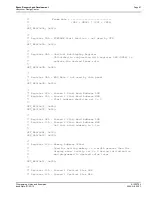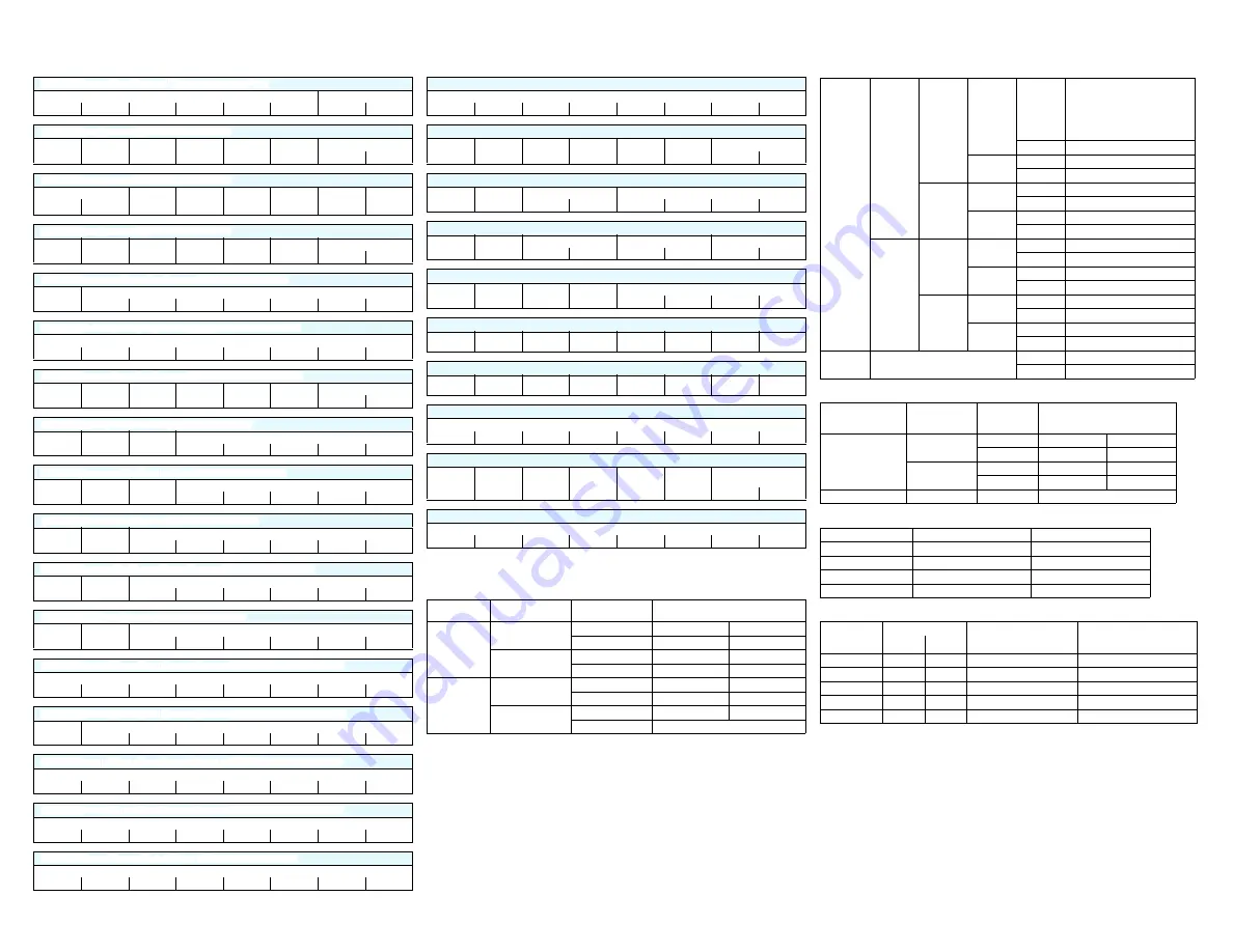
S1D13704 Register Summary
X26A-R-001-03
Page 1
01/02/12
Notes
1 These bits are used to identify the S1D13704 at power on / reset.
2 IO addresses are relative to the beginning of display memory.
3 Gray Shade/Color Mode Selection
4 Panel Data Format
5 High Performance Selection
6 Power Save Mode Selection
7 Look-Up Table Access
REG[00h] R
EVISION
C
ODE
R
EGISTER
1
IO address = FFE0h
2
, RO
Product Code = 000110
Revision Code = 00
Bit 5
Bit 4
Bit 3
Bit 2
Bit 1
Bit 0
Bit 1
Bit 0
REG[01h] M
ODE
R
EGISTER
0
IO address = FFE1h, RW
TFT/STN
Dual/Single Color/Mono
3
FPLine
Polarity
FPFrame
Polarity
Mask
FPSHIFT
Data Width
4
Bit 1
Bit 0
REG[02h] M
ODE
R
EGISTER
1
IO address = FFE2h, RW
Bit-Per-Pixel
3
High
5
Performance
Input Clock
Div (CLKI/2)
Display
Blank
Frame
Repeat
Hw Video
Invert
Enable
Software
Video Invert
Bit 1
Bit 0
REG[03h] M
ODE
R
EGISTER
2
IO address = FFE3h, RW
Look-Up
Table Bypass
n/a
n/a
n/a
LCDPWR
Override
Hardware
PS Enable
Sw Power Save
6
Bit 1
Bit 0
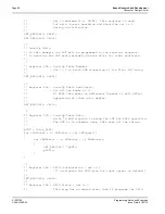
REG[04h] H
ORIZONTAL
P
ANEL
S
IZE
R
EGISTER
IO address = FFE4h, RW
n/a
Horizontal Panel Size = 8(REG + 1)
Bit 6
Bit 5
Bit 4
Bit 3
Bit 2
Bit 1
Bit 0
REG[05h] V
ERTICAL
P
ANEL
S
IZE
R
EGISTER
(LSB)
IO address = FFE5h, RW
Vertical Panel Size = (REG[05h], REG[06h]) + 1
Bit 7
Bit 6
Bit 5
Bit 4
Bit 3
Bit 2
Bit 1
Bit 0
REG[06h] V
ERTICAL
P
ANEL
S
IZE
R
EGISTER
(MSB)
IO address = FFE6h, RW
n/a
n/a
n/a
n/a
n/a
n/a
Vertical Panel Size
Bit 9
Bit 8
REG[07h] FPL
INE
S
TART
P
OSITION
IO address = FFE7h, RW
n/a
n/a
n/a
FPLine Start Position = 8(REG[07h] + 2)
Bit 4
Bit 3
Bit 2
Bit 1
Bit 0
REG[08h] H
ORIZONTAL
N
ON
-D
ISPLAY
P
ERIOD
IO address = FFE8h, RW
n/a
n/a
n/a
Horizontal Non-Display Period = 8(REG + 4)
Bit 4
Bit 3
Bit 2
Bit 1
Bit 0
REG[09h] FPF
RAME
S
TART
P
OSITION
IO address = FFE9h, RW
n/a
n/a
FPFrame Start Position
Bit 5
Bit 4
Bit 3
Bit 2
Bit 1
Bit 0
REG[0Ah] V
ERTICAL
N
ON
-D
ISPLAY
P
ERIOD
R
EGISTER
IO address = FFEAh, RW
Vert Non-
Disp Status
n/a
Vertical Non-Display Period
Bit 5
Bit 4
Bit 3
Bit 2
Bit 1
Bit 0
REG[0Bh] MOD R
ATE
R
EGISTER
IO address = FFEBh, RW
n/a
n/a
MOD Rate
Bit 5
Bit 4
Bit 3
Bit 2
Bit 1
Bit 0
REG[0Ch] S
CREEN
1 S
TART
W
ORD
A
DDRESS
R
EGISTER
(LSB)
IO address = FFECh, RW
Screen 1 Start Word Address = (REG[0Ch], REG[0Dh])
Bit 7
Bit 6
Bit 5
Bit 4
Bit 3
Bit 2
Bit 1
Bit 0
REG[0Dh] S
CREEN
1 S
TART
W
ORD
A
DDRESS
R
EGISTER
(MSB)
IO address = FFEDh, RW
reserved
Screen 1 Start Word Address
Bit 14
Bit 13
Bit 12
Bit 11
Bit 10
Bit 9
Bit 8
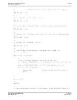
REG[0Fh] S
CREEN
2 S
TART
W
ORD
A
DDRESS
R
EGISTER
(LSB)
IO address = FFEFh, RW
Screen 2 Start Word Address = (REG[0F], REG[10h])
Bit 7
Bit 6
Bit 5
Bit 4
Bit 3
Bit 2
Bit 1
Bit 0
REG[10h] S
CREEN
2 S
TART
W
ORD
A
DDRESS
R
EGISTER
(MSB)
IO address = FFF0h, RW
Screen 2 Start Word Address
Bit 15
Bit 14
Bit 13
Bit 12
Bit 11
Bit 10
Bit 9
Bit 8
REG[12h] M
EMORY
A
DDRESS
O
FFSET
R
EGISTER
IO address = FFF2h, RW
Memory Address Offset
Bit 7
Bit 6
Bit 5
Bit 4
Bit 3
Bit 2
Bit 1
Bit 0
REG[13h] S
CREEN
1 V
ERTICAL
S
IZE
R
EGISTER
(LSB)
IO address = FFF3h, RW
Screen 1 Vertical Size = (REG[13h], REG[14h])
Bit 7
Bit 6
Bit 5
Bit 4
Bit 3
Bit 2
Bit 1
Bit 0
REG[14h] S
CREEN
1 V
ERTICAL
S
IZE
R
EGISTER
(MSB)
IO address = FFF4h, RW
n/a
n/a
n/a
n/a
n/a
n/a
Screen 1 Vertical Size
Bit 9
Bit 8
REG[15h] L
OOK
-U
P
T
ABLE
A
DDRESS
R
EGISTER
7
IO address = FFF5h, RW
n/a
n/a
RGB Index
Look-Up Table Address
Bit 1
Bit 0
Bit 3
Bit 2
Bit 1
Bit 0
REG[16h] L
OOK
-U
P
T
ABLE
B
ANK
S
ELECT
R
EGISTER
IO address = FFF6h, RW
n/a
n/a
Red Bank Select
Green Bank Select
Blue Bank Select
Bit 1
Bit 0
Bit 1
Bit 0
Bit 1
Bit 0
REG[17h] L
OOK
-U
P
T
ABLE
D
ATA
R
EGISTER
IO address = FFF7h, RW
n/a
n/a
n/a
n/a
Look-Up Table Data
Bit 3
Bit 2
Bit 1
Bit 0
REG[18h] GPIO C
ONFIGURATION
C
ONTROL
R
EGISTER
IO address = FFF8h, RW
n/a
n/a
n/a
GPIO4 Pin
IO Config
GPIO3 Pin
IO Config
GPIO2 Pin
IO Config
GPIO1 Pin
IO Config
GPIO0 Pin
IO Config
REG[19h] GPIO S
TATUS
/ C
ONTROL
R
EGISTER
IO address = FFF9h, RW
n/a
n/a
n/a
GPIO4 Pin
IO Status
GPIO3 Pin
IO Status
GPIO2 Pin
IO Status
GPIO1 Pin
IO Status
GPIO0 Pin
IO Status
REG[1Ah] S
CRATCH
P
AD
R
EGISTER
IO address = FFFAh, RW
Scratch Pad Register
Bit 7
Bit 6
Bit 5
Bit 4
Bit 3
Bit 2
Bit 1
Bit 0
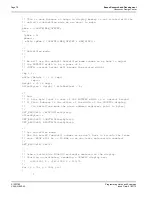
REG[1Bh] S
WIVEL
V
IEW
M
ODE
R
EGISTER
IO address = FFFBh, RW
SwivelView
Mode En.
SwivelView
Mode Sel.
n/a
n/a
n/a
reserved
SwivelView Mode PCLK
Select
Bit 1
Bit 0
REG[1Ch] L
INE
B
YTE
C
OUNT
R
EGISTER
IO address = FFFCh, RW
Line Byte Count
Bit 7
Bit 6
Bit 5
Bit 4
Bit 3
Bit 2
Bit 1
Bit 0
Color/Mono
REG[01] bit 5
Bit-Per-Pixel Bit 1
REG[02] bit 7
Bit-Per-Pixel Bit 0
REG[02] bit 6
Display Mode
1
0
0
2 Colors
1 Bit-Per-Pixel
1
4 Colors
2 Bit-Per-Pixel
1
0
16 Colors
4 Bit-Per-Pixel
1
256 Colors
8 Bit-Per-Pixel
0
0
0
2 Gray Shade
1 Bit-Per-Pixel
1
4 Gray Shade
2 Bit-Per-Pixel
1
0
16 Gray Shade
4 Bit-Per-Pixel
1
reserved
TFT/STN
REG[01]
bit 7
Color/
Mono
REG[01]
bit 5
Dual/
Single
REG[01]
bit 6
Data
Width
Bit 1
REG[01]
bit 1
Data
Width
Bit 0
REG[01]
bit 0
Function
0
0
0
0
0
Mono Single 4-bit LCD
1
Mono Single 8-bit LCD
1
0
reserved
1
reserved
1
0
0
reserved
1
Mono Dual 8-bit LCD
1
0
reserved
1
reserved
1
0
0
0
Color Single 4-bit LCD
1
Color Single 8-bit LCD Format 1
1
0
reserved
1
Color Single 8-bit LCD Format 2
1
0
0
reserved
1
Color Dual 8-bit LCD
1
0
reserved
1
reserved
1
don’t care
0
9 bit TFT Panel
1
12 bit TFT Panel
High Performance
Bit-Per-Pixel
Bit 1
REG[02] bit 7
Bit-Per-Pixel
Bit 0
REG[02] bit 6
Display Modes
0
0
0
MClk = PClk/8
1 bit-per-pixel
1
MClk = PClk/4
2 bit-per-pixel
1
0
MClk = PClk/2
4 bit-per-pixel
1
MClk = PClk
8 bit-per-pixel
1
X
X
MClk = PClk
Power Save Bit 1
Power Save Bit 0
Mode
0
0
Software Power Save Mode
0
1
reserved
1
0
reserved
1
1
Normal Operation
Color/Mono
REG[01h]
bit 5
REG[15h]
Look-Up Table Selected
Pointer Sequence
bit 5
bit 4
0
X
X
Green/Gray Look-Up Table
G[n], G[n+1], G[n+2]...
1
0
0
Auto-Increment
R[n], G[n], B[n] R[n+1], G[n+1],...
1
0
1
Red Look-Up Table
R[n], R[n+1], R[n+2]...
1
1
0
Green/Gray Look-Up Table
G[n], G[n+1], G[n+2]...
1
1
1
Blue Look-Up Table
B[n], B[n+1], B[n+2]...
S1D13704 Register Summary
X26A-R-001-03
*

