Epson Research and Development
Page 15
Vancouver Design Center
Hardware Functional Specification
S1D13704
Issue Date: 01/02/08
X26A-A-001-04
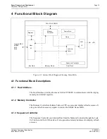
4 Functional Block Diagram
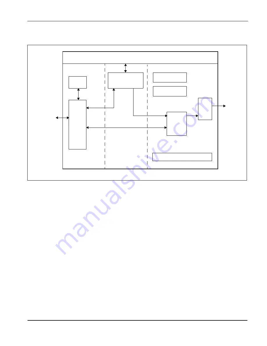
Figure 4-1: System Block Diagram Showing Data Paths
4.1 Functional Block Descriptions
4.1.1 Host Interface
The Host Interface provides the means for the CPU/MPU to communicate with the display
memory and internal registers.
4.1.2 Memory Controller
The Memory Controller arbitrates between CPU accesses and display refresh accesses. It
also generates the necessary signals to control the SRAM frame buffer.
4.1.3 Sequence Controller
The Sequence Controller controls data flow from the Memory Controller through the Look-
Up Table and to the LCD Interface. It also generates memory addresses for display refresh
accesses.
LCD
Memory
Controller
20k x 16-bit SRAM
LCD
Clocks
Power Save
Register
Sequence Controller
Look-Up
I/F
Generic MPU
MC68K
SH-3
Host
I/F
Bus Clock
Memory Clock
Pixel Clock
Table
SH-4
*

