Page 20
Epson Research and Development
Vancouver Design Center
S1D13704
Hardware Functional Specification
X26A-A-001-04
Issue Date: 01/02/08
5.2.2 LCD Interface
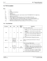
RD#
I
76
CS
Input
This pin has multiple functions.
• For SH-3/SH-4 mode, this pin inputs the read signal
(RD#).
• For MC68K #1, this pin must be tied to IO V
DD
.
• For MC68K #2, this pin inputs the bus size bit 1 (SIZ1).
• For Generic #1, this pin inputs the read command for the
lower data byte (RD0#).
• For Generic #2, this pin inputs the read command (RD#).
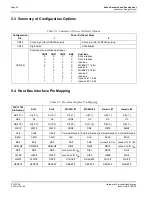
See “Host Bus Interface Pin Mapping” for summary.
WAIT#
O
2
TS2
High
Impedance
This pin has multiple functions.
• For SH-3 mode, this pin outputs the wait request signal
(WAIT#).
• For SH-4 mode, this pin outputs the device ready signal
(RDY#).
• For MC68K #1, this pin outputs the data transfer
acknowledge signal (DTACK#).
• For MC68K #2, this pin outputs the data transfer and
size acknowledge bit 1 (DSACK1#).
• For Generic #1, this pin outputs the wait signal (WAIT#).
• For Generic #2, this pin outputs the wait signal (WAIT#).
See “Host Bus Interface Pin Mapping” for summary.
RESET#
I
73
CS
0
Active low input to set all internal registers to the default state
and to force all signals to their inactive states.
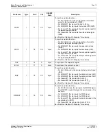
Pin Name
Type
Pin #
Cell
RESET#
State
Description
FPDAT[7:0]
O
30, 31, 32,
33, 34, 35,
36, 37
CN3
0
Panel Data
FPDAT[10:8]
O,
I/O
24, 25, 26
CN3
Input
These pins have multiple functions.
• Panel Data bits [10:8] for TFT/D-TFD panels.
• General Purpose Input/Output pins GPIO[3:1].
These pins should be connected to IO V
DD
when unused.
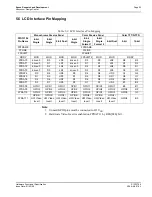
See “LCD Interface Pin Mapping” for summary.
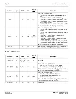
FPDAT11
O,
I/O
23
CN3
Input
This pin has multiple functions.
• Panel Data bit 11 for TFT/D-TFD panels.
• General Purpose Input/Output pin GPIO4.
• Inverse Video select pin.
This pin should be connected to IO V
DD
when unused. See
“LCD Interface Pin Mapping” for summary.
FPFRAME
O
39
CN3
0
Frame Pulse
Pin Names
Type
Pin #
Cell
RESET#
State
Description
*


