Page 10
Epson Research and Development
Vancouver Design Center
S1D13704
Interfacing to the NEC VR4102™ Microprocessor
X26A-G-008-05
Issue Date: 01/02/12
3 S1D13704 Host Bus Interface
This section is a summary of the host bus interface modes available on the S1D13704 and
offers some detail on the Generic #2 host bus interface used to implement the interface to
the VR4102.
3.1 Bus Interface Modes
The S1D13704 implements a 16-bit interface to the host microprocessor which may operate
in one of several modes compatible with most of the popular embedded microprocessor
families. Six bus interface modes are supported:
• Hitachi SH-4.
• Hitachi SH-3
• Motorola MC68000 (using Upper Data Strobe/Lower Data Strobe).
• Motorola MC68020/MC68030/MC683xx (using Data Strobe/DSACKx).
• Generic #1 (Chip Select, plus individual Read Enable/Write Enable for each byte).
• Generic #2 (External Chip Select, shared Read/Write Enable for high byte, individual
Read/Write Enable for low byte).
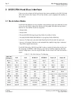
The S1D13704 latches CNF[2:0] and BS# to allow selection of the host bus interface on
the rising edge of RESET#. After releasing reset, the bus interface signals assume their
selected configuration. The following table shows the functions of each host bus interface
signal.
Table 3-1: Host Bus Interface Pin Mapping
S1D13704
Pin Names
SH-3
SH-4
MC68K #1
MC68K #2
Generic #1
Generic #2
AB[15:1]
A[15:1]
A[15:1]
A[15:1]
A[15:1]
A[15:1]
A[15:1]
AB0
A0
A0
LDS#
A0
A0
A0
DB[15:0]
D[15:0]
D[15:0]
D[15:0]
D[31:16]
D[15:0]
D[15:0]
WE1#
WE1#
WE1#
UDS#
DS#
WE1#
BHE#
CS#
CSn#
CSn#
External Decode
External Decode External Decode
External Decode
BCLK
CKIO
CKIO
CLK
CLK
BCLK
BCLK
BS#
BS#
BS#
AS#
AS#
connect to V
SS
connect to IO V
DD
RD/WR#
RD/WR#
RD/WR#
R/W#
R/W#
RD1#
connect to IO V
DD
RD#
RD#
RD#
connect to IO V
DD
SIZ1
RD0#
RD#
WE0#
WE0#
WE0#
connect to IO V
DD
SIZ0
WE0#
WE#
WAIT#
WAIT#
RDY#
DTACK#
DSACK1#
WAIT#
WAIT#
RESET#
RESET#
RESET#
RESET#
RESET#
RESET#
RESET#
*

